RBSE Solutions for Class 12 Physics Chapter 14 Semiconductor Electronics: Materials, Devices and Simple Circuits
Rajasthan Board RBSE Solutions for Class 12 Physics Chapter 14 Semiconductor Electronics: Materials, Devices and Simple Circuits Textbook Exercise Questions and Answers.
Rajasthan Board RBSE Solutions for Class 12 Physics in Hindi Medium & English Medium are part of RBSE Solutions for Class 12. Students can also read RBSE Class 12 Physics Important Questions for exam preparation. Students can also go through RBSE Class 12 Physics Notes to understand and remember the concepts easily. Browsing through wave optics important questions that include all questions presented in the textbook.
RBSE Class 12 Physics Solutions Chapter 14 Semiconductor Electronics: Materials, Devices and Simple Circuits
RBSE Class 12 Physics Semiconductor Electronics: Materials, Devices and Simple Circuits Textbook Questions and Answers
Question 14.1.
In an n-type silicon, which of the following statement is true?
(a) Electrons are majority carriers and trivalent atoms are the dopants.
(b) Electrons are minority carriers and pentavalent atoms are the dopants.
(c) Holes are minority carriers and pentavalent atoms are the dopants.
(d) Holes are majority carriers and trivalent atoms are the dopants.
Answer:
(c) Holes are minority carriers and pentavalent atoms are the dopants.

Question 14.2.
Which of the statements given in Exercise 14.1 is true for p-type semiconductors?
(a) Electrons are majority carriers and trivalent atoms are the dopants.
(b) Electrons are minority carriers and pentavalent atoms are the dopants.
(c) Holes are minority carriers and pentavalent atoms are the dopants.
(d) Holes are majority carriers and trivalent atoms are the dopants.
Answer:
(d) Holes are majority carriers and trivalent atoms are the dopants.
Question 14.3.
Carbon, silicon and germanium have four valence electrons each. These are characterised by valence and conduction bands separated by energy band gap respectively equal to (Eg)C, (Eg)Si, and (Eg)Ge. Which of the following sfatments is true?
(a) (Eg)Si < (Eg)Ge < (Eg)C
(b) (Eg)C < (Eg)Ge < (Eg)Si
(c) (Eg)C > (Eg)Si > (Eg)Ge
(d) (Eg)C = (Eg)Si = (Eg)Ge.
Answer:
(c) (Eg)C > (Eg)Si > (Eg)Ge
Question 14.4.
In an unbiased p-n junction, holes diffuse from the p-region to n-region because
(a) free electrons in the n-region attract them
(b) they move across the junction by the potential difference
(c) hole concentration in p-region is more as compared to n-region
(d) All the above.
Answer:
(c) hole concentration in p-region is more as compared to n-region
Question 14.5.
When a forward bias is applied to a p-n junction, it
(а) raises the potential, barrier
(b) reduces the majority carrier current to zero
(c) lowers the potential barrier
(d) None of the above.
Answer:
(c) lowers the potential barrier
Question 14.6.
For transistor action, which of the following statements are correct?
(а) Base, emitter and collector regions should have similar size and doping concentrations
(b) The base region must be very thin and lightly doped
(c) The emitter junction is forward biased and collector junction is reverse biased.
(d) Both the emitter junction as well as the collectpr junction are forward biased
Answer:
(b) The base region must be very thin and lightly doped
(c) The emitter junction is forward biased and collector junction is reverse biased.
Question 14.7.
For transistor amplifier, the voltage gain.
(a) remains constant for all frequencies
(b) is high at high and low frequencies
(c) is low at high and low frequencies and constant in the middle frequency range
(d) None of the above.
Answer:
(c) is low at high and low frequencies and constant in the middle frequency range
Question 14.8.
In half-wave rectification, what is the output frequency if the input frequency is 50 Hz? What is the output frequency of a full wave rectifier for the same input frequency?
Answer:
Given input frequency = 50 Hz.
Output frequency
For Half wave rectifier = 50 Hz
For full wave rectifier = 50 x 2
= 100 Hz.
Question 14.9. For a C.E. transistor amplifier, the audio signal voltage across the collector resistance of 2 kΩ is 2V. Suppose the current amplification factor of the transistor is 100, find the input signal voltage and base current, if the base resistance is 1 kΩ.
Answer:
Given ß = 100, Ri = 1 kΩ,
R0 = 2 kΩ
Voltage gain,
A = Current gain x Resistance gain
= 100 x \(\frac{\mathrm{R}_0}{\mathrm{R}_i}\) = 100 x \(\frac{2}{1}\) = 200
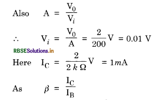
∴ IB = \(\frac{\mathrm{I}_{\mathrm{C}}}{\beta}=\frac{1 m \mathrm{~A}}{100}\) = 0.01 mA = 10 µA.
Question 14.10.
Two amplifiers are connected one after the other in series (cascaded). The first amplifier has a voltage gain of 10 and the second has a voltage gain of 20. If the input signal is 0.01 volt, calculate the output a.c. signal.
Answer:
Given AV1 =10 and AV2 = 20
Vi1 = 0.01V
So voltage gain of 1st amplifier
AV1 = \(\frac{\mathrm{V}_{01}}{\mathrm{~V}_{i 1}} \)
∴ V01 = Vi1 AV1
or V01 = 0.01 X 10 = 0.1 V
And voltage gain of 2nd amplifer
AV2 = \(\frac{V_{02}}{V_{01}}\)
0r V02 = V01 AV2
= 0.1 x 20
or V02 = 2V.
Question 14.11.
A p-n photodiode is fabricated from a semiconductor with band gap of 2.8 eV. Can it detect a wavelength of 6000 nm?
Answer:
Band gap Eg = 2.8 eV
Energy band gap corresponding to wavelength 6000 nm is given by
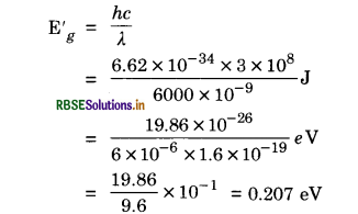
Since Eg' < Eg, so it cannot detect a wavelength of 6000 nm.
ADDITIONAL EXERCISES
Question 14.12.
The number of silicon atoms per m3 in 5 x 10²². This is doped simultaneously with 5 x 10²² atoms per m3 of Arsenic and 5 x 10²⁰ per m3 atoms of Indium. Calculate the number of electrons and holes. Given that ni = 1.5 x 10¹⁶ m-3. Is the material n-type or p-type?
Answer:
Given n = 5 x 10²² m-3
ND = 5 x 10²² m-3
NA = 5 x 10²⁰ m-3
= 0.05 x 10²² m-3
ni = 1.5 x 10¹⁶ m-3.
Since ne - nh = ND - NA .....................(1)
And ne - nh = ni2 ....................(2)
So ne + nh = \(\sqrt{\left(n_e-n_h\right)^2+4 n_e n_h}\)
Using Eq. (1) and (2), we get
ne + nh = \(\sqrt{\left(\mathrm{N}_{\mathrm{D}}-\mathrm{N}_{\mathrm{A}}\right)^2+4 n_i^2}\) .........................(3)
Adding (1) and (3), we get
ne = \(\frac{1}{2}\left[\left(\mathrm{~N}_{\mathrm{D}}-\mathrm{N}_{\mathrm{A}}\right)+\sqrt{\left(\mathrm{N}_{\mathrm{D}}-\mathrm{N}_{\mathrm{A}}\right)^2+4 n_i^2}\right]\)
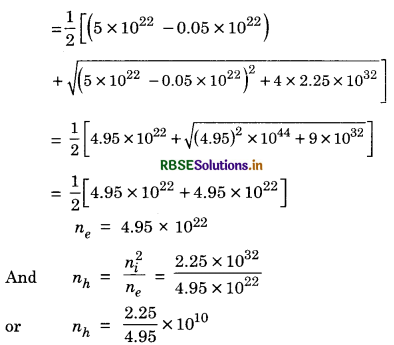
nh = 4.55 x 10⁹
Since ne >> nh, so the material is n-type.
Question 14.13.
In an intrinsic semiconductor the energy gap Eg is 1.2 eV. Its hole mobility is independent of temperature. What is the ratio between conductivity at 600 K and that at 300 K? Assume that the temperature dependence of intrinsic carrier concentration ni is expressed as:
ni = n0 exp\([\frac{-\mathrm{E}_{\mathrm{g}}}{2 \mathrm{k}_{\mathrm{B}} \mathrm{T}}]\)
when n0 is a constant.
Answer:
Since µe > µh and for the intrinsic semiconductor ne = nh = ni can be written as
σe = µene
Using the equation for ni given in the problem
σ = eµen0 exp.\(\left[\frac{-\mathrm{E}_g}{k_{\mathrm{B}} \mathrm{T}}\right]\)
All the pre-exponential terms are assumed independence of temperature. We can put a constant.
σ0 = eµen0
and express the conductivity.
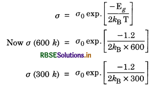
Takin gkB = 8.62 x 10⁻⁵ eVK-1 and solving, we get
\(\frac{\sigma(600 \mathrm{~K})}{\sigma(300 \mathrm{~K})}\) ≈ 1 x 10⁵
This shows that the conductivity of an intrinsic semiconductor is greatly influenced by temperature.
Question 14.14.
In a p-n junction diode the current I can be expressed.
I = I0 \(\left[\exp \cdot\left(\frac{e \mathrm{~V}}{\mathrm{k}_{\mathrm{B}} \mathrm{T}}\right)-\mathbf{i}\right]\)
where I0 is called the reverse saturation current, V is the voltage across the diode and is positive for forward bias and negative for reverse bias and I is the current through the diode, KB is the Boltzmann’s constant (8.6 x 10⁻⁵ eV/K) and T is the absolute temperature. If for a diode I0 = 5 x 10-12 A and T = 300 K, then
(а) What will be the forward current at a forward voltage of 0.6 V?
(b) What will be the increase in the current if the voltage across the diode is increased to 0.7 V?
(c) What is the dynamic resistance?
(d) What will be current if reverse bias voltage changes from IV to 2 V?
Answer:
Given that
I = I0 \(\left[\exp \cdot\left(\frac{e \mathrm{~V}}{\mathrm{k}_{\mathrm{B}} \mathrm{T}}\right)-\mathbf{i}\right]\)
I0 = 5 x 10-12 A; T = 300 K and kB = 8.6 x 10⁻⁵ e V/K
(a) For V = 0.6 V
\(\frac{e \mathrm{~V}}{k_{\mathrm{B}} \mathrm{T}}=\frac{e \times 0.6 \mathrm{~V}}{8.6 \times 10^{-5}}(e \mathrm{~V} / \mathrm{K})(300 \mathrm{~K})=\frac{100}{4.3}\)
∴ exp. \(\left(\frac{100}{4.3}\right)\) = 1.2585 x 10¹⁰
∴ I = 5 x 10-12 x 1.2585 x 1010 = 0.0629 A
(b) V = 0.7 V
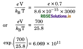
I = 5 x 10-12 x 6.069 x 1011 = 3.0349 A
Increase in current = 3.0349 - 0.0629 = 2.927 A
(c) Dynamic Resistance
= \(\frac{\delta \mathrm{V}}{\delta \mathrm{I}}=\frac{0.1}{2.927}\) = 0.0336 Ω
(d) For reverse bias V = -1 volt
I = I0 [e (-38.76) - 1] = -5 x 10-12 A
For V = -2V
I = 5 x 10-12 A
Change in current is zero.
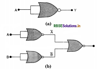
Question 14.15.
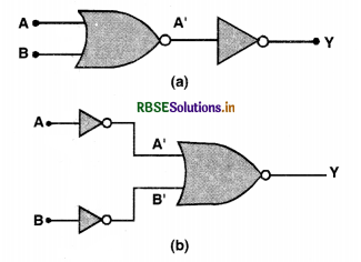
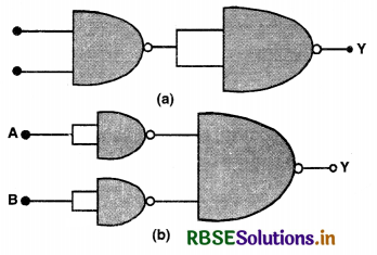
You are given two circuits as shown in Fig. TBQ 14.15. Show that circuit (a) acts as OR gate while the circuit
(b) acts as AND gate.
Answer:
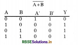
The truth table of circuit (a) is:
|
A |
B |
A’ |
Y |
|
0 |
0 |
1 |
0 |
|
0 |
1 |
0 |
0 |
|
1 |
0 |
0 |
0 |
|
1 |
1 |
0 |
1 |
Thus we find that the circuit (a) operation of OR gate is performing the operation of OR gate.
|
A |
B |
A’ |
B’ |
Y |
|
0 |
0 |
1 |
1 |
0 |
|
0 |
1 |
1 |
0 |
0 |
|
1 |
0 |
0 |
1 |
0 |
|
1 |
1 |
0 |
0 |
1 |
Thus we find that the circuit (b) is performing the operation of AND gate.
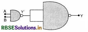
Question 14.16.
Write the truth table for a NAND gate connected as given in Fig. TBQ 14.16.
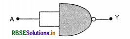
Answer:
The truth table of the given NAND gate connected as shown in Fig. TBQ 14.16 (b) is
Question 14.17.
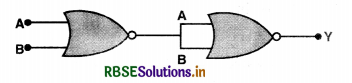
You are given two circuits as shown in Fig. TBQ 14.17 which consist of NAND gates. Identify the logic operation carried out by the two circuits.
Answer:
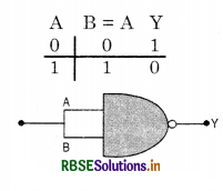
(a) The circuit (a) is AND gate, because the circuit can be represented as:
So the truth table is :
|
A |
B |
Y’ =\( \overline{\mathrm{A} \cdot \mathrm{B}}\) |
Y = \(\overline{\mathrm{A} \cdot \mathrm{B}}\) |
|
0 |
0 |
1 |
0 |
|
0 |
1 |
1 |
0 |
|
1 |
0 |
1 |
0 |
|
1 |
1 |
0 |
1 |
Hence the circuit (c) behaves like an AND gate
(b) The circuit (d) is OR gate, because the circuit can be represented as:
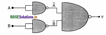
So the truth table is :
|
A |
B |
\(\overline{\mathrm{A}}\) |
\(\overline{\mathrm{B}}\) |
Y = \(\overline{\overline{\mathrm{A}} \cdot \overline{\mathrm{B}}}\) = A + B |
|
0 |
0 |
1 |
1 |
0 |
|
0 |
1 |
1 |
0 |
1 |
|
1 |
0 |
0 |
1 |
1 |
|
1 |
1 |
0 |
0 |
1 |
Hence the circuit (b) behaves like an OR gate.
Question 14.18.
Write the truth table for circuit given in the figure TBQ 14.18 (a) consisting of NOR gates and identify the logic operation (OR, AND, NOT) which this (circuit is performing.
Hint. A = 0, B = 1, then A and B inputs of second NOR gate will be 0 and hence Y = 1. Similarly work out the values of Y for other combinations of A and B. Compare with truth of OR, AND, NOT gates and find the correct one.
Answer:
The truth table is shown in Fig. TBQ 14.18 (b)
Thus we find that the circuit is performing the operation of OR gate.
Question 14.19.
Write the truth table for the circuit given in the following figures consisting of NOR gates only. Identify the logic operations (OR, AND, NOT) performed by the two circuits.
Answer:
In Fig. TBQ 14.19 (a), two inputs A and B are given to a NOR gate and its output is given to the input of a NOT gate.
So the truth table is:
|
A |
B |
Y = \(\overline{\mathrm{A}+\mathrm{B}}\) |
|
0 |
0 |
1 |
|
1 |
1 |
0 |
This is the truth table of OR gate, Hence Fig. TBQ 14.19 (a) acts as an OR gate.
In Fig. TBQ 14.19 (b), inputs A and B are given to two NOT gates and their output is given to a NOR gate.
So the truth table is:
|
A |
B |
\(\overline{\mathrm{A}}\) |
\(\overline{\mathrm{B}}\) |
Y = \(\overline{\overline{\mathrm{A}}+\overline{\mathrm{B}}} \overline{\bar{A}}+\overline{\bar{B}}\) = A.B |
|
0 |
0 |
1 |
1 |
0 |
|
0 |
1 |
1 |
0 |
0 |
|
1 |
0 |
0 |
1 |
0 |
|
1 |
1 |
0 |
0 |
1 |
This is the truth table of an AND gate, hence Fig. TBQ 14.19 (b) acts as an AND gate.
SELECTED EXEMPLAR PROBLEMS
MCQ I. (with one correct option)
Question 14.1.
The conductivity of a semiconductor increases with increase in temperature because
(a) number density of free current carriers increases.
(b) relaxation time increases.
(c) both number density of carriers and relaxation time increase.
(d) number density of current carriers increases, relaxation time decreases but effect of decrease in relaxation time is much less than increase in number density.
Answer:
(d) n increases, r decreases but decrease in r is much less than increase in n.
Question 14.2.
In Fig. EP 14.2 V0 is the potential barrier across a p-n junction, when no battery is connected across the junction
(a) 1 and 3 both correspond to forward bias of junction
(b) 3 corresponds to forward bias of junction and 1 corresponds to reverse bias of junction.
(c) 1 corresponds to forward bias and 3 corresponds to reverse bias of junction.
(d) 3 and 1 both correspond to reverse bias of junction.
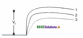
Answer:
(b) A p-n junction during forward bias opposes the potential barrier and during reverse bias, it supports the potential barrier.
Question 14.3.
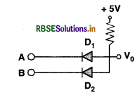
In Fig. EP 14.3. assuming the diodes to be ideal.
(a) D1 is forward biased and D2 is reverse biased and hence current flows from A to B
(b) D2 is forward biased and D1 is reverse biased and hence no current flows from B to A and vice versa.
(c) D1 and D2 are both forward biased and hence current flows from A to B.
(d) D1 and D2 are both reverse biased and hence no current flows from A to B and vice versa
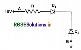
Answer:
(d) Here both the diodes are reverse biased as it is clear from the figure.
Question 14.4.
A 220 V A.C. supply is connected between points A and B (Fig. EP 14.4). What will be the potential difference V across the capacitor?
(a) 220V.
(b) 110 V
(c) 0V.
(d) 220 \(\sqrt{2}\) V.
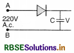
Answer:
(d) A p-n junction conducts only during positive half, and the potential across the capacitor is equal to the peak voltage of a.c.
i.e. E0 = Ev \(\sqrt{2}\) = 220 \(\sqrt{2}\) V
Question 14.5.
Hole is
(a) an anti-particle of electron.
(b) a vacancy created when an electron leaves a covalent bond.
(c) absence of free electrons.
(d) an artificially created particle.
Answer:
(b) (Knowledge based question.)
Question 14.6.
The output of the given circuit in Fig. EP 14.6.
(а) would be zero at all times.
(b) would be like a half wave rectifier with positive cycles in output.
(c) would be like a half wave rectifier with negative cycles in output.
(d) would be like that of a full wave rectifier.
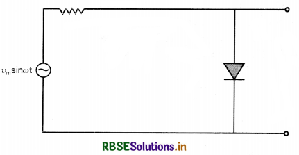
Answer:
(c)
The p-n junction is forward biased during +ve half of input ac and its resistance is low, and large potential difference will appear across the resistance connected in series. And voltage across p-n junction is zero.
The p-n junction is reverse biased during -ve half of input a.c. and its resistance is high, and will be more than resistance connected in series and there will be voltage across the p-n junction with negative cycle in output. Hence the circuit would be half wave rectifier with negative cycle in output.
Question 14.7.
In the circuit shown in Fig. EP 14.7, if the diode forward voltage drop is 0.3 V, the voltage difference between A and B is
(а) 1.3 V
(b) 2.3 V
(c) 0
(d) 0.5 V
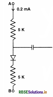
Answer:
(b) V - 0.3 = RI
V - 0.3 = [(5 + 5) x 103] x 0.2 x 10-3
= 10 x 103 x 0.2 x 10-3
= 2
or V = 2 + 0.3 = 2.3 volt.
Question 14.8.
Truth table for the given circuit (Fig. EP 14.8.) is
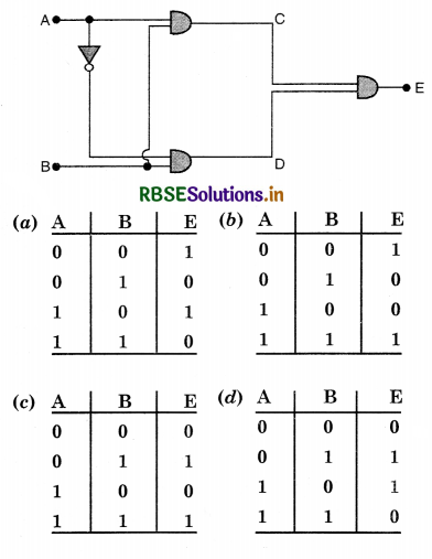
Answer:
(c) Here C = A B & D = \(\overline{\mathrm{A}}\). B
And E = C + D = A.B + \(\overline{\mathrm{A}}\) B
Truth table is
|
A |
B |
\(\overline{\mathrm{A}}\) |
C = A.B |
D = \(\overline{\mathrm{A}}\) B |
E = C + D |
|
0 |
0 |
1 |
0 |
0 |
0 |
|
0 |
1 |
1 |
0 |
1 |
1 |
|
1 |
0 |
0 |
0 |
0 |
0 |
|
1 |
1 |
0 |
1 |
0 |
1 |
MCQ II. (with more than one correct options)
Question 14.9.
When an electric field is applied across a semiconductor
(а) electrons move from lower energy level to higher energy level in the conduction band.
(b) electrons move from higher energy level to lower energy level in the conduction band.
(c) holes in the valence band move from higher energy level to lower energy level.
(d) holes in the valence band move from lower energy level to higher energy level.
Answer:
(a), (c) Knowledge based question.
Question 14.10.
Consider a npn transistor with its base-emitter junction forward biased and collector base junction reverse biased. Which of the following statements are true?
(a) Electrons cross over from emitter to collector.
(b) Holes move from base to collector.
(c) Electrons move from emitter to base.
(d) Electrons from emitter move out of base without going to the collector.
Answer:
(a), (c) Knowledge based question.
Question 14.11.
Figure EP 14.11 shows the transfer characteristics of a base-biased CE transistor. Which of the following statements are true?
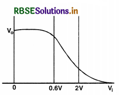
(a) At Vi = 0.4 V, transistor is in active state.
(b) At Vi = 1V, it can be used as an amplifier.
(c) At Vi = 0.5 V, it can be used as a switch turned off.
(d) At Vi = 2.5 V, it can be used as a switch turned on.
Answer:
(b), (c), (d)
At Vi = 0.4 V, there is no current and transistor is in cut-off state.
Question 14.12.
In a npn transistor circuit, the collector current is 10 mA. If 95 percent of the electrons emitted reach the collector, which of the following statements are true?
(a) The emitter current will be 8 mA.
(b) The emitter current will be 10.53 mA.
(c) The base current will be 0.53 mA.
(d) The base current will be 2 mA.
Answer:
(b), (c)
Given Ic = 10 mA
And Ic = \(\frac{95}{100}\) Ie
or Ie = \(\frac{100}{95}\) Ic = \(\frac{10 \times 100}{95}\) = 10.53 mA
Ib = Ie - Ic = 10.53 - 10 = 0.53 mA
Question 14.13.
In the depletion region of a diode
(a) there are no mobile charges
(b) equal number of holes and electrons exist, making the region neutral.
(c) recombination of holes and electrons has taken place.
(d) immobile charged ions exist.
Answer:
(a), (b), (d)
Electrons and holes are not present in depletion layer hence their recombination cannot take place.
Question 14.14.
What happens during regulation action of a Zener diode?
(a) The current and voltage across the Zener remain fixed.
(b) The current through the series resistance (Rg.) changes.
(c) The Zener resistance is constant.
(d) The resistance offered by the Zener changes.
Answer:
(b), (d)
During regulation action of a Zener diode, the current through resistance changes and the resistance offered by the Zener changes.
Question 14.15.
To reduce the ripples in a rectifier circuit with capacitor filter
(a) RL should be increased.
(b) input frequency should be decreased.
(c) input frequency should be increased.
(d) capacitors with high capacitance should be used.
Answer:
(a), (c), (d)
Since ripple factor with capacitor filter is:
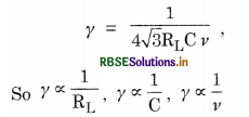
So to reduce γ, Increase RL, C and v.
Question 14.16.
The breakdown in a reverse biased p-n junction diode is more likely to occur due to
(a) large velocity of the minority charge carriers if the doping concentration is small.
(b) large velocity of the minority charge carriers if the doping concentration is large.
(c) strong electric field in a depletion region if the doping concentration is small.
(d) strong electric field in a depletion region if the doping concentration is large.
Answer:
(a), (d)
Very Short Answer Type Questions
Question 14.17.
Wliy are elemental dopants for Silicon or Germanium usually chosen from group XIII or group XV?
Answer:
The dopant should be such that the size of the dopant atom should not distort the pure semi-conductor lattice structure and it should easily contributes a charge carrier, which are provided by group XIII or group XV elements.
Question 14.18.
Sn, C, and Si, Ge are all group XIV elements. Yet, Sn is a conductor, C is an insulator while Si and Ge are semiconductors. Why?
Answer:
The energy gap for Sn is 0 eV, for C is 5.4 eV and Si is 1.1 eV and for Ge is 0.7 eV. So Sn is a conductor, C is an insulator, Si and Ge are semi-conductors.
Question 14.19.
Can the potential barrier across a p-n junction be measured by simply connecting a voltmeter across the junction?
Answer:
No, because the resistance of the voltmeter should be very high as compared to the junction resistance and resistance of the junction is nearly infinite.
Question 14.20.
Draw the output waveform across the resistor (Fig. EP 14.20).
Question 14.21.
The amplifiers X, Y and Z are connected in series. If the voltage gains of X, Y and Z are 10, 20 and 30, respectively and the input signal is 1 mV peak value, then what is the output signal voltage (peak value)
(i) if d.c. supply voltage is 10V?
(ii) if d.c. supply voltage is 5V?
Answer:
(i) If d.c. supply voltage is 10V, the output signal voltage
∆V0 = 10 x 20 x 30 x 10-3 = 6V
(ii) If d.c. supply voltage is 5 V, then output peak will not exceed 5 V. So V0 = 5 V.
Question 14.22.
In a CE transistor amplifier there is a current and voltage gain associated with the circuit. In other words there is a power gain. Considering power a meausre of energy, does the circuit violate conservation of energy?
Answer:
There is no violation of conservation of energy because the extra power required for amplified output is obtained from d.c. source.
Short Answer Type Questions
Question 14.23.
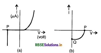
(i) Name the type of a diode whose characteristics are shown in Fig. EP 14.23 (a) and Fig. EP 14.23 (b).
(ii) What does the point P in Fig. EP 14.23 (a) represent?
(iii) What does the points P and Q in Fig. EP 14.23 (b) represent?
Answer:
(i) Zener junction diode and solar cell
(ii) Zener breakdown voltage
(iii) Q-Short circuit current and P-open circuit voltage.
Question 14.24.
Three photodiodes D1, D2 and D3 are made of semiconductors having band gaps of 2.5 eV, 2 eV and 3eV, respectively. Which ones will be able to detect light of wavelength 6000 Å?
Answer:
Energy of incident light
E = hv = \(\frac{h c}{\lambda}=\frac{6.62 \times 10^{-34} \times 3 \times 10^8}{6000 \times 10^{-10}}\) = 2 eV
So only diode D2 will detect this radiation, because the incident radiation photon should be greater than the band gap.
Question 14.25.
If the resistance, R1 is increased (Fig. EP 14.25), how will the readings of the ammeter and voltmeter change?
Answer:
From Fig. EP 14.25 (a) we find that
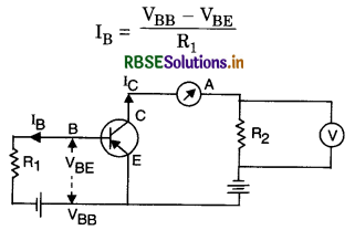
If R1 is increased, IB will decrease.
Also IC = ßIB
As IB decreased, IC also decreased. So there is decrease in ammeter and voltmeter readings.
Question 14.26.
Two car garages have a common gate which needs to open automatically when a car enters either of the garages or cars enter both. Devise a circuit that resembles this situation using diodes for this situation.
Answer:
The circuit is an OR gate as shown in the figure.
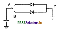
The gate output is given by the truth table.
|
A |
B |
Y = A + B |
|
0 |
0 |
0 |
|
0 |
1 |
1 |
|
1 |
0 |
1 |
|
1 |
1 |
1 |
Question 14.27.
How would you set up a circuit to obtain NOT gate using a transistor?
Answer:
The circuit diagram using a transistor to obtain NOT gate is as shown in the figure
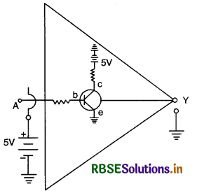
Truth table
|
A |
Y |
|
0 |
1 |
|
1 |
0 |
Question 14.28.
Explain why elemental semi-conductor cannot be used to make visible LEDs.
Answer:
The band gap of elemental semiconductors is such that the emissions are in IR region and not in visible region as required in LEDs.
Question 14.29.
Write the truth table for the circuit shown in Fig. EP 14.29. Name the gate that the circuit resembles.
Answer:
|
A |
B |
Y = V0 |
|
0 |
0 |
0 |
|
0 |
1 |
0 |
|
1 |
0 |
0 |
|
1 |
1 |
1 |
The circuit resembles AND gate
Question 14.30.
A Zener of power rating 1 W is to be used as a voltage regulator. If Zener has a breakdown of 5V and it has to regulate voltage which fluctuated between 3V and 7 V, what should be the value of Rs for safe operation (Fig. EP 14.30)?
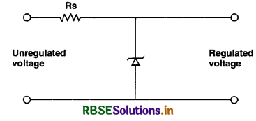
Answer:
Iz max = \(\frac{\mathrm{P}}{\mathrm{V}_{\mathrm{z}}}=\frac{1}{5}\) = 0.2 A = 200 mA
Rs = \(\frac{\mathrm{V}_{\mathrm{s}}-\mathrm{V}_{\mathrm{z}}}{\mathrm{I}_{\mathrm{z} \max }}=\frac{2}{0.2}\) = 10 Ω
Long Answer Type Questions
Question 14.31.
If each diode in Fig. EP 14.31 has a forward bias resistance of 25 Ω and infinite resistance in reverse bias, what will be the values of the currents I1, I2, I3 and I4?
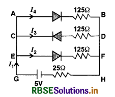
Answer:
Here diode in branch AB and EF are forward biased and diode in branch CD is reverse biased (infinite resistance).
∴ I3 = 0
Resistance in branch AB and EF all each = 125 + 25 = 150 Ω
These two resistances all in parallel.
So their equivalent resistance is \(\frac{150}{2}\) = 75 Ω
∴ Total resistance in the circuit
= 75 + 25 = 100 Ω
∴ Current I1 = \(\frac{5}{100}\) = 0.05 A
Since I1 = I2 + I3 + I4
or I1 = I2 + I4 ..............(i) [∵ I3 = 0]
Since resistance in branch AB and EF is the same
So I4 = I2
So eq. (i) becomes
I1 = 2I2
or I2 = \(\frac{\mathrm{I}_1}{2}=\frac{0.05}{2}\) = 0.025 A
And I4 = 0.025 A
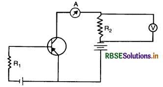
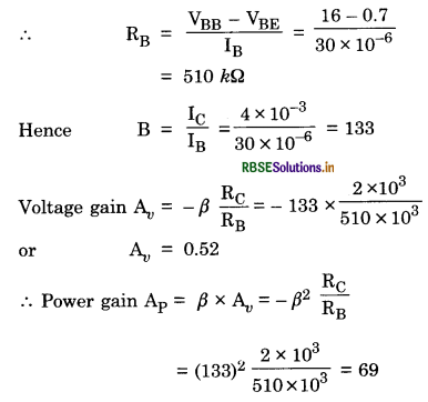
Question 14.34.
Consider the circuit arrangement shown in Fig. EP 14.34 (a) for studying input and output characteristics of npn transistor in CE configuration.
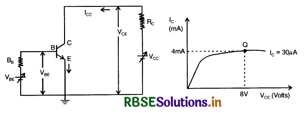
Select the values of RB and RC for a transistor whose VBE = 0.7 V, so that the transistor is operating at point Q as shown in the characteristics graph in Fig. EP 14.34 (b).
Given that the input impedance of the transistor is very small and VCC = VBB = 16 V, also find the voltage gain and power gain of circuit making appropriate assumptions.
Answer:
Here VBE = 0.7 V, VCC = VBB = 16 V
(From the graph)
VCE = 8 V
IC = 4 mA = 4 x 10⁻³ A
and IB = 30 µA = 30 x 10-6 A
∴ VCC = IC RC + VCE
or R = \(\frac{\mathrm{V}_{\mathrm{CC}}-\mathrm{V}_{\mathrm{CE}}}{\mathrm{I}_{\mathrm{C}}}\)
= \(\frac{16-8}{4 \times 10^{-3}}\) = 2 kΩ
As VBB = IBRB + VBE
Question 14.35.
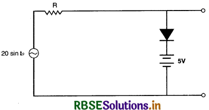
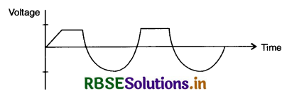
Assuming the ideal diode, draw the output waveform for the circuit given in Fig. EP 14.35. Explain the waveform.
Answer:
When input voltage is equal or less than 5V, the diode will be reverse biased offering high resistance and diode appears in open circuit. And input waveform is passed to output terminal. So the sine wave input is to dip off all positive going portion above 5V. When input is more than 5V, the diode is conducting and there will be no voltage beyond 5V as the voltage beyond 5V will appear across R. When input voltage is -ve there will be opposition to 5 V battery in p-n junction. Due to it, reverse bias voltage decreases and appear across output. When input voltage is more than -5V, the diode will be reverse biased and junction diode appears in open circuit as shown in the given figure.
Question 14.36.
Suppose a ‘n’-type wafer is created by doping Si crystal having 5 x 1028 atoms/m3 with 1 ppm concentration of As. On the surface 200 ppm Boron is added to create ‘P' region in this wafer. Considering ni = 1.5 x 10¹⁶ m-3
(i) Calculate the densities of the charge carriers in the n and p regions
(ii) Comment which charge carriers would contribute largely for the reverse saturation current when diode is reverse biased.
Answer:
(i) In ‘n' region: number of e- is due to As
∴ ne = ND = 1 x 10-6 x 5 x 1028 = 5 x 10²² m-3.
The minority carriers (hole) in n type water is
nh = \(\frac{n_i^2}{n_e}=\frac{\left(1.5 \times 10^{16}\right)^2}{5 \times 10^{22}}=\frac{2.25 \times 10^{32}}{5 \times 10^{22}}\)
or nh = 0.45 x 10¹⁰ m-3.
Similarly, when boron is implanted a p-type is created with holes
nh = NA = 200 x 10-6 x 5 x 1028 = 1 x 1025 m-3
Minority carriers created in p-type wafer is
ne = \(\frac{n_i^2}{n_h}=\frac{2.25 \times 10^{32}}{1 \times 10^{25}}\) = 2.25 x 10⁷ m-3
(ii) When p-n junction is reverse biased, the minority carrier holes of n-region wafer (nh = 0.45 x 10¹⁰ m-3) would contribute more to the reverse saturation current than minority electrons (ng = 2.25 x 10⁷ m-3) of p-region water.
Question 14.39.
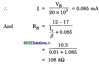
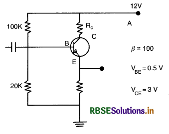
For the transistor circuit shown in Fig. EP 14.39 evaluate VE, RB, RE given Ic = 1 mA, VCE = 3V, VBE = 0.5 V and VCC = 12 V. ß = 100.
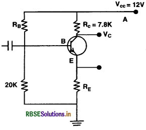
Answer:
Collector current is almost equal to emitter current
i.e. Ic = IE and Rc = 7.8 kΩ
RE = 9 - Rc = 1.2 kΩ
∴ VE = 1.2 V
VB = VE + VBE = 1.7 V
Question 14.40.
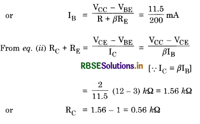
In the circuit shown in Fig. EP 14.40, find the value of Rc.
Answer:
IE = IC + IB and IC = ßIB ...................(i)
ICRC + VCE + IERE = VCC ....................(ii)
R IB + VBE + IERE = VCC ..........................(iii)
From eq. (iii), IE = IC = ßIB
From eq. (iii), IB (R + ßRE) = VCC - VBE

- RBSE Class 12 Physics Notes Chapter 2 स्थिर वैद्युत विभव तथा धारिता
- RBSE Class 12 Physics Notes Chapter 3 विद्युत धारा
- RBSE Class 12 Physics Notes Chapter 4 गतिमान आवेश और चुंबकत्व
- RBSE Class 12 Physics Notes Chapter 5 चुंबकत्व एवं द्रव्य
- RBSE Class 12 Physics Notes Chapter 6 वैद्युत चुंबकीय प्रेरण
- RBSE Class 12 Physics Notes Chapter 7 प्रत्यावर्ती धारा
- RBSE Class 12 Physics Notes Chapter 8 वैद्युतचुंबकीय तरंगें
- RBSE Class 12 Physics Notes Chapter 9 किरण प्रकाशिकी एवं प्रकाशिक यंत्र
- RBSE Class 12 Physics Notes Chapter 10 तरंग-प्रकाशिकी
- RBSE Class 12 Physics Notes Chapter 11 विकिरण तथा द्रव्य की द्वैत प्रकृति
- RBSE Class 12 Physics Notes Chapter 12 परमाणु