RBSE Class 12 Physics Important Questions Chapter 14 Semiconductor Electronics: Materials, Devices and Simple Circuits
Rajasthan Board RBSE Class 12 Physics Important Questions Chapter 14 Semiconductor Electronics: Materials, Devices and Simple Circuits Important Questions and Answers.
Rajasthan Board RBSE Solutions for Class 12 Physics in Hindi Medium & English Medium are part of RBSE Solutions for Class 12. Students can also read RBSE Class 12 Physics Important Questions for exam preparation. Students can also go through RBSE Class 12 Physics Notes to understand and remember the concepts easily. Browsing through wave optics important questions that include all questions presented in the textbook.
RBSE Class 12 Physics Chapter 14 Important Questions Semiconductor Electronics: Materials, Devices and Simple Circuits
Multiple Choice Questions
Question 1.
With fall of temperature, the forbidden energy gap of a semiconductor:
(A) increases
(B) decreases
(C) remains unchanged
(D) sometime increase and sometimes decreases.
Answer:
(C) remains unchanged

Question 2.
The relation between number of free electrons (n) in a semiconductor and temperature (T) is given by:
(A) n ∝ T
(B) n ∝ T2
(C) n ∝ \(\sqrt{\mathrm{T}}\)
(D) n ∝ T3/2.
Answer:
(D) n ∝ T3/2.
Question 3.
The typical ionisation energy of a donor in silicon is:
(A) 10.00 eV
(B) 1.0 eV
(C) 0.1 eV
(D) 0.001 eV.
Answer:
(C) 0.1 eV
Question 4.
When a semiconductor is heated, its resistance:
(A) decreases
(B) increases
(C) remains unchanged
(D) nothing is definite.
Answer:
(A) decreases
Question 5.
The energy band gap is maximum in:
(A) Metals
(B) Super conductors
(C) Insulators
(D) Semiconductors.
Answer:
(C) Insulators
Question 6.
Zener diode is used for:
(A) Amplification
(B) Rectification
(C) Stabilization
(D) All of them.
Answer:
(C) Stabilization
Question 7.
PN junction is:
(A) ohmic resistance
(B) non-ohmic resistance
(C) negative resistance
(D) positive resistance.
Answer:
(B) non-ohmic resistance
Question 8.
The depletion region of PN junction has a thickness of the order of:
(A) 10-12
(B) 10-6 m
(C) 1 mm
(D) 1 cm.
Answer:
(B) 10-6 m
Question 9.
Current gain in common-base configuration is less than 1, because:
(A) Ie < Ip
(B) Ip < Ie
(C) Ic < Ie
(D) Ie < Ic.
Answer:
(C) Ic < Ie
Question 10.
Majority charge carriers in p-type semiconductor are:
(A) Holes
(B) Electrons
(C) Holes and electrons
(D) None of these.
Answer:
(A) Holes
Question 11.
Boron is added as impurity to silicon, the resultant semiconductor is:
(A) n-type semiconductor
(B) p-type semiconductor
(C) n-type conductor
(D) None of these.
Answer:
(B) p-type semiconductor
Question 12.
Depletion layer consists of:
(A) electrons
(B) immobile ions
(C) mobile ions
(D) Both A and B.
Answer:
(B) immobile ions
Question 13.
A n-type semiconductor is:
(A) Neutral
(B) Negatively charged
(C) Positively charged
(D) None of these.
Answer:
(A) Neutral
Question 14.
A device which converts d.c. into a.c. is called:
(A) Rectifier
(B) Oscillator
(C) Amplifier
(D) Modulator.
Answer:
(B) Oscillator
Question 15.
Radiowaves of constant amplitude can be generated with:
(A) Filter
(B) Rectifier
(C) FET
(D) Oscillator.
Answer:
(D) Oscillator.
Question 16.
A p-n junction diode can be used as:
(A) Rectifier
(B) Modulator
(C) Demodulator
(D) Amplifier.
Answer:
(A) Rectifier & (C) Demodulator
Question 17.
Holes are charge carrets in:
(A) Intrinsic semiconductor
(B) p-type semiconductor
(C) n-type semiconductor
(D) Ionic solids.
Answer:
(B) p-type semiconductor
Question 18.
The number of electrons in the valence shell of the pure semiconductor is:
(A) 6
(B) 5
(C) 4
(D) 3.
Answer:
(C) 4
Question 19.
At zero kelvin, a piece of Germanium behaves as:
(A) semiconductor
(B) insulator
(C) good conductor
(D) superconductor.
Answer:
(B) insulator
Question 20.
To obtain a p-type germanium semiconductor, it must be doped with
(A) arsenic
(B) antimony
(C) indium
(D) phosphorus.
Answer:
(C) indium
Question 21.
A pure semiconductor behaves slightly as a conductor at:
(A) High temperature
(B) Room temperature
(C) Low temperature
(D) None of the above.
Answer:
(A) High temperature
Question 22.
The relation between base current (Ib), emitter current (Ie) and collector current (Ic) for common base transistor is:
(A) Ib = Ie + Ic
(B) Ic = Ib + Ie
(C) Ie = Ib + Ic
(D) None of these.
Answer:
(C) Ie = Ib + Ic
Question 23.
In N-type semi-conductor, relation between number of electron density (ne) and number of hole density (nh) is:
(A) ne >> nh
(B) nh >> ne
(C) nh = ne
(D) None of these.
Answer:
(A) ne >> nh
Question 24.
With the increase in temperature, the resistance of semi-conductors:
(A) Decreases
(B) Increases
(C) Remains same
(D) None of these.
Answer:
(A) Decreases
Question 25.
When arsenic is added an impurity to silicon, the resulting material is:
(A) n-type semiconductor
(B) n-type semiconductor
(C) intrinsic semiconductor
(D) none of these.
Answer:
(A) n-type semiconductor
Question 26.
Which of the following elements is a semiconductor?
(A) Na
(B) Ba
(C) Sr
(D) Ge.
Answer:
(D) Ge.
Question 27.
In binary number system 111 represent:
(A) One
(B) Three
(C) Seven
(D) One hundred and eleven.
Answer:
(C) Seven
Question 28.
Which of these is universal logic gate?
(A) OR
(B) AND
(C) NAND
(D) NOT.
Answer:
(C) NAND
Fill in the blanks
Question 1.
A semiconductor doped with pentavalent impurity is called .................................. semiconductor.
Answer:
N-type.
Question 2.
The lowest unfilled energy band formed just above valance band is called .................................. band.
Answer:
conduction.
Question 3.
The width of depletion layer is about .................................. m.
Answer:
10-6.
Question 4.
In a transistor base is always .................................. and .................................. doped.
Answer:
Thin, lightly.
Question 5.
A transistor acts as an amplifier, when it operatea in .................................. state.
Answer:
active.
Question 6.
A transistor can be used as a switch by operating it in its .................................. state or .................................. state.
Answer:
cut off, saturation.
Question 7.
A transistor can be used as an .................................. and ..................................
Answer:
amplifier, oscillator.
Question 8.
The reverse bias applied to a junction diode .................................. its potential barrier.
Answer:
raises.
Question 9.
Zener diode is always operated at .................................. bias.
Answer:
reverse.
Question 10.
An oscillator gives an a.c. output signal without requiring any .................................. signal.
Answer:
input.
Very Short Answer Type Questions
Question 1.
Define energy gap.
Answer:
The difference in the extreme energy levels of a forbidden band is called energy gap (Eg).
Question 2.
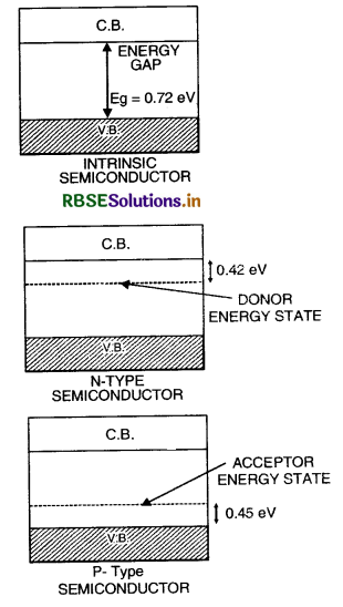
Give values of energy gap (Eg) for a semiconductor and for an insulator.
Answer:
(i) For a semiconductor, Eg = 1 eV
(ii) For an insulator, Eg = 6 eV.
Question 3.
Define hole.
Answer:
A place vacated by an electron, is called a hole, it is associated with a positive charge.
Question 4.
How does a semiconductor behave at OK?
Answer:
It behaves like an insulator.
Question 5.
Define semiconductor.
Answer:
A solid is a semiconductor if the energy gap between the valence band and a conduction band is small (0.1 to 1 eV).
Question 6.
What is doping?
Answer:
The process of adding impurity to a pure semiconductor in a controlled manner is called doping.
Question 7.
Doping of silicon with indium leads to which type of semiconductor?
Answer:
When silicon is doped with indium we get p-type semiconductor.
Question 8.
What is n-type semiconductor?
Answer:
A semiconductor which has been doped with pentavalent impurity is called n-type semiconductor.
Question 9.
What is p-type semiconductor?
Answer:
A semiconductor which has been doped with trivalent impurity is called p-type semiconductor.
Question 10.
Why is a semiconductor damaged by a strong current?
Answer:
Semiconductors are very sensitive to heat. When a strong current is passed through them, a good amount of heat produced and the bonds of semiconductor break resulting in a avalanche of electrons. Thus the crystal gets damaged on passing very heavy current.
Question 11.
What is an energy band in solids?
Answer:
An energy band consists of a large number of discrete but closely packed energy levels.
Question 12.
What is valence band?
Answer:
The highest energy band occupied by the valence electrons is called valence band.
Question 13.
What is conduction band?
Answer:
The empty band is called conduction band.
Question 14.
What is forbidden band?
Answer:
The separation between conduction band and a valence band is called forbidden band.
Question 15.
What is the value of band gap and in semiconductor?
Answer:
In Si the energy gap is 1.1 eV and in Ge it is 0.7 eV.
Question 16.
What is fermi level?
Answer:
The highest occupied energy level, in conduction band, at 0 K is called fermi level.
Question 17.
Is the number of electrons and holes equal in an n-type semiconductor?
Answer:
No, the number of free electrons is more than number of holes.
Question 18.
When the temperature of a semi-conductor is increased, what changes are expected in the majority charge carriers ratio?
Answer:
On increasing the temperature the number of minority carriers increases and number of majority carriers remain the same. Hence the ratio of majority and minority carriers decreases.
Question 19.
What is a p-n junction?
Answer:
A p-n junction is a crystal of Si or Ge doped in such a manner that half of it is p-type semiconductor and other half is n-type semiconductor.
Question 20.
What is the size of depletion layer in a p-n junction?
Answer:
It is about 10-6 m.
Question 21.
What is junction potential barrier?
Answer:
The potential barrier is the difference of potential between junction ends of two types of semiconductor.
Question 22.
Why is junction potential barriers so called?
Answer:
Since it prevnts free charge carriers from entering the depletion layer by themselves, so it is called potential barrier.
Question 23.
How does a p-n junction break down?
Answer:
When large inverse bias is applied, the breakdown of p-n junction takes place due to excessive heating.
Question 24.
Define Zener voltage.
Answer:
Zener voltage is the maximum reverse voltage applied to p-n junction at which an excessive reverse current flows.
Question 25.
What is this reverse current due to?
Answer:
This reverse current is due to the condition of thermally generated electron-hole pair within p-type and n-type materials. Because some covalent bonds always break down due to normal heat energy of the cyrstal molecules.
Question 26.
What happens if forward bias is made very high?
Answer:
If forward bias is made very high, the junction will be destroyed due to overheating.
Question 27.
What is maximum power rating of p-n junction diode?
Answer:
It is the maximum power that can be dissipated at the junction without damaging it. The power dissipated at the junction is equal to the product of junction current and the voltage across the junction.
Question 28.
What is knee voltage?
Answer:
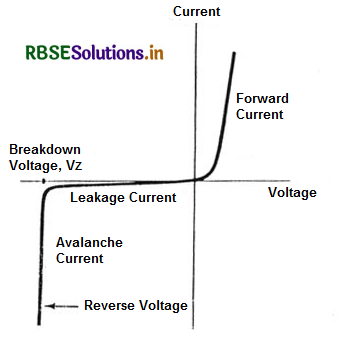
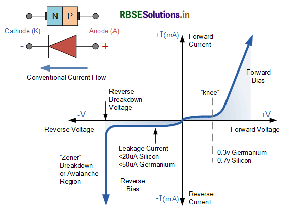
It is the forward voltage at which the current through the junction starts to increase rapidly. Knee voltage for Ge diode is 0.3 V and for Si diode it is 0.7 V. It may be noted that in order to get useful current through a p-n junction, the applied voltage must be more than the knee voltage.
Question 29.
What do you mean by power dissipation in the zener diode?
Answer:
Power dissipation in the diode is the product of V2 and reverse current I2 with maximum power ranging from 150 mW to 50 W.
Question 30.
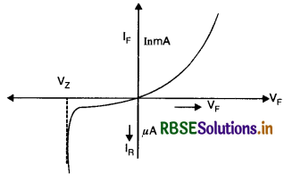
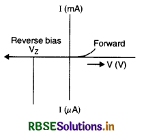
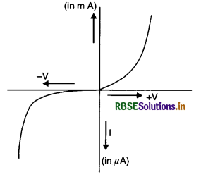
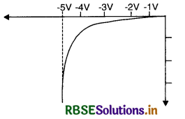
Draw the voltage characteristic of a Zener diode?
Answer:
Question 31.
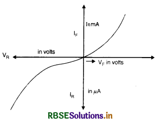
Draw the voltage current characteristic of a p-n diode bias.
Answer:
Question 32.
How does the width of depletion layer of p-n junction vary, if the reverse bias applied to it decrases?
Answer:
The width of the depletion layer decreases with the decrease in the reverse bias.
Question 33.
What is breakdown voltage range of a zener diode?
Answer:
By varying the doping level, it is possible to produce zener diodes with breakdown voltage from 2 V to 200 V.
Question 34.
What is the most common application of a zener diode?
Answer:
The most common application of a zener diode is in the voltage stabilizing or regulator circuits.
Question 35.
How does zener diode act in forward bias conditions?
Answer:
In forward bias conditions, a zener diode acts like a conventional p-n junction diode.
Question 36.
How can you test in a simple way whether transistor is spoiled or not?
Answer:
Connect BE to a cell and an ammeter. Note the current, reverse the connections and note the current again. If current in two cases is widely different, the BE side is fine otherwise it is spoiled. Similarly check BC side.
Question 37.
Which one will you prefer, a common base or a common emitter amplifier?
Answer:
Common emitter is preferred to common base since its current gain is more than common base type amplifier.
Question 38.
Why transistor is so called?
Answer:
By biasing the BE forward and CB in reverse, we decrease the resistance of BE and increase the resistance of CB circuit. Thus we transfer resistance from BE to CB and hence it is called transfer resistor or transistor.
Question 39.
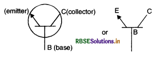
Draw the symbolic diagram of an n-p-n transistor.
Answer:
Symbolic diagrams of an n-p-n transistor are as given in figures.
Question 40.
What is an amplifier?
Answer:
An amplifier is a circuit consisting of at least one transistor which is used to increase the voltage or power of alternating form.
Question 41.
What is an oscillator?
Answer:
It is an electronic device which converts direct current into alternating current of very high frequency.
Question 42.
What type of impurity is added to obtain n-type semiconductor?
Answer:
Pentavalent impurity i.e. As or Sb.
Question 43.
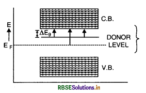
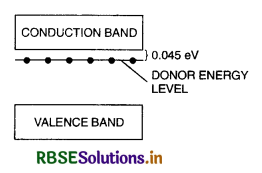
Draw energy-band diagram for n-type extrinsic semiconductor.
Answer:
It is shown in the figure.
Question 44.
How does the width of the depletion layer of p-n junction diode change with decrease in reverse bias?
Answer:
It decreases.
Question 45.
State the reason, why a photodiode is usually operated at reverse bias?
Answer:
Because the fractional change in reverse bias current due to minority charge carriers is much more than over the majority charge carriers in forward bias. Hence photo diodes are used to measure the intensity in reverse bias.
Question 46.
At what temperature would an intrinsic semiconductor behave like a perfect insulator?
Answer:
At 0 K.
Question 47.
How does a sample of an n-type semiconductor electrically neutral though it has an excess negative charge carriers?
Answer:
Because the excess charge gets balanced by an equal and opposite charge of the ionised core in the lattice.
Question 48.
State the factor, which controls:
(i) wavelength of light, and (ii) intensity of light emitted by a LED.
Answer:
(i) Wavelength of light emitted depends on the nature of semiconductor, band gap and nature of impurity.
(ii) The intensity of light emitted depends on the extent of forward biasing.
Question 49.
Zener diodes have the higher dopant densities as compared to ordinary p-n junction diodes. How does it affect the
(i) width of the depletion layer?
(ii) Junction field?
Answer:
(i) Width of the depletion layer will be small.
(ii) Junction field will be more.
Question 50.
Carbon and silicon are known to have similar lattice structures. However, the four bonding electrons of carbon are present in second orbit while those of silicon are present in its third orbit. How does this difference result in a difference in their electrical conductivities?
Answer:
The ionisation energy of silicon gets considerably reduced as compared to carbon, thus silicon (act as semiconductor) becomes a much better conductor of electricity than carbon (which is an insulator).
Question 51.
How does the energy gap in an intrinsic semiconductor vary, when doped with a pentavalent impurity?
Answer:
The energy gap will be reduced.
Question 52.
The energy gaps in the energy band diagrams of a conductor, semiconductor and insulator are E1, E2 and E3. Arrange them in increasing order. Answer:
For conductor, E1 = 0, For semiconductor E2 ≃ 1 eV. and for insulator E3 ≥ 3eV.
So E1 < E2 < E3.
Question 53.
Draw energy band diagram of an n- type semiconductor.
Answer:
Question 54.
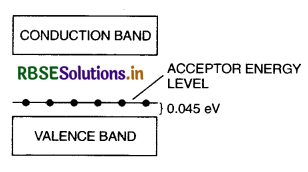
Draw energy band diagram of a p-type semiconductor.
Answer:
Question 55.
Draw the voltage-current characteristics of a zener diode.
Answer:
Voltage-current characteristics of a zener diode is shown in Fig. VSAQ 55
Question 56.
Draw the voltage-current characteristics of a p-n diode bias.
Answer:
Voltage-current characteristics of a p-n diode is shown in Fig. VSAQ 56.
Question 57.
Which type of biasing gives a semiconductor diode very high resistance?
Answer:
Reverse biasing
Question 58.
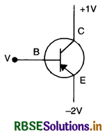
In Fig. VSAQ 58 is (i) the emitter and (ii) the collector forward or reverse biased?
Answer:
In the given figure VSAQ 58 is a p-n-p transistor, so
(i) emitter is reverse biased and
(ii) the collector is forward biased.
Question 59.
In a semiconductor the concentration of electrons is 8 x 1013 cm-3 and that of holes is 5 x 102 cm-3. Is it a p-type or n-type semiconductor?
Answer:
Here ne > nh, hence it is n-type semi-conductor.
Question 60.
Give the ratio of the number of holes and number of conductor electrons in an intrinsic semiconductor.
Answer:
1 : 1.
Question 61.
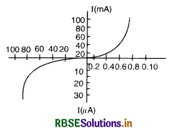
Figure VSAQ 61 shows the I - V characteristic of a given device. Name the device and write where it is used.
Answer:
The name of the device is zener diode. It is used as voltage regulator.
Short Answer Type Questions
Question 1.
What do you mean by valence band, conduction band and forbidden gap?
Answer:
Valence band. The highest band occupied by the valence electrons is called valence band.
Conduction band. The empty band is called conduction band.
Forbidden gap. The separation between conduction band and valence band is called forbidden energy gap.
Question 2.
What do you mean by semiconductors?
Answer:
Those substances which have their conductivity intermediate between conductors and insulators are called semiconductors i.e. the resistivity at room temperature is in the range of 10-5 to 104 Ωm. The forbidden gap for C, Ge and Si at 0 K is 5.48 eV, 0.74 eV and 1.17 eV and at 300 k, 5.47 eV, 0.66 eV and 1.12 eV respectively. Thus in terms of energy band, semiconductor may be defined as those materials which have almost an empty conduction band and almost filled valence band with a very narrow energy gap (≅ eV) separating the two.
Question 3.
What is an intrinsic semi-conductor? How can this material be converted into (i) p-type, (ii) n-type extrinsic semiconductor? Explain with the help of energy band diagrams.
Answer:
Intrinsic semiconductor. A pure semiconductor having no impurity in it is called as intrinsic semiconducter.
An intrinsic semiconductor doped by a suitable impurity is called an extrinsic semiconductor and is of two types:
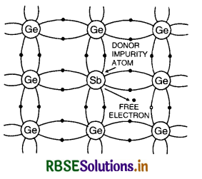
(i) n-type semiconductor. When an intrinsic semiconductor say Si or Ge is doped by an impurity of an atom of + 5 valency element, we get a n-type semiconductor. This pentavalent impurity is called donor impurity (As, Sb, P etc.)
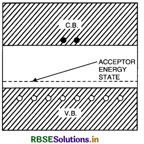
(ii) p-type semiconductor. When an intrinsic semiconductor say Si or Ge is doped by an impurity of an atom of +3 valency element, we get a p-type semiconductor. This trivalent impurity is called acceptor impurity (In, Al, B etc.).
Energy level diagrams:
Question 4.
What are extrinsic semiconductors? Describe p-type semiconductor?
Answer:
Extrinsic semiconductors: A doped semiconductor or a sein iconductor with impurity atoms is called an extrinsic semiconductor.
p-Type semiconductors
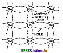
In p-type Ge. If we dope intrinsic Ge, with a controlled amount of trivalent atoms, say indium (In or boron B or aluminium Al) Group III, which has three valence electrons, impurity atom will occupy places of some Ge atoms and there will be one incomplete covalent bond with a neighbouring Ge atom, due to the deficiency of an electron. This is completed by taking an electron from one of the Ge-Ge bonds, thus completing the In-Ge bond. This
makes In ionized (negatively charged), and creates a ‘hole’ or an electron deficiency in Ge. The trivalent atoms are called acceptor atoms and this extrinsic semiconductor is known as p-type.
Question 5.
What are extrinsic semiconductors? Describe N-type semiconductor?
Answer:
Extrinsic semiconductors: A doped semiconductor or a sein iconductor with impurity atoms is called an extrinsic semiconductor.
n-Type semiconductor.
The conductivity of intrinsic semiconductor is zero at absolute zero and very small at ordinary temperatures. Germanium has 4.52 x 10²² atoms per cm3. An addition of only one impurity atom per million Ge atom, is sufficient to give desired conductivity to it. The process of deliberately adding suitable impurity atom to the intrinsic semiconductor is called Doping (the impure semiconductor is called a doped semiconductor). If we dope intrinsic Ge with a controlled amount of pentavalent atoms, say antimony Sb or phosphorus P, which has five valence electrons, the atoms of the impurity element will substitute the Germanium atoms (Fig. 14.89(a)). Four of the five valence electrons is comparatively free to move. The pentavalent atoms are called the donor atoms because they donate electrons to the host crystal extrinsic semiconductor are called n-type. On giving up their fifth electron, the donor atoms become positively charged. However, the material remains electrically neutral as a whole.
Question 6.
Distinguish between conductor and semiconductor on the basis of their energy bands.
Answer:
Semiconductors
The energy and structure of a semi conductor is shown in Fig. LAQ 2 (b) It is similar to that of an insulator but with a comparatively small energy gap of about 1 eV. At. absolute zero of temperature, the conduction band of semiconductor is totally empty, and all the energy states in the valence band are filled. The absence of electrons in the conduction band at absolute zero does not allow current to flow under the influence of an electric field. Therefore, they are insulators at low temperatures. However, at room temperature, some valence electrons acquire thermal energy greater than the energy gap Eg and move to the conduction band where they are free to move under the influence of even a small electric field. Common examples of semiconductors are silicon (14), Germanium (32) with energy gap of about (1.12 eV) and 0.75 eV respectively. The gap (band) that separates conduction and valence band is called Forbidden Band.
Metals (Conductors)
The energy band structure of a metal is shown schematically in Fig. LAQ 2 (c). The last occupied band of energy levels is only partially filled:
The available electrons occupy, one by one (Pauli exclusion principle) the lowest levels. This leaves part of the band (called conduction band un occupied. The highest energy level occupied at absolute zero by electrons is partially filled conduction band. is called Fermi level and the corresponding energy is called Fermi energy.
When an electric field is applied, electrons gain energy (about 10-8 eV). They can be excited to empty energy levels immediately about the Fermi level and some of the electrons are accelerated in the direction of the field. Thus electric current is conducted through the conductors.
Question 7.
Why the resistivity of semi-conductors lies between the conductors and insulators?
Answer:
In covalent solids (semiconductors) some of the covalent bonds break down and electrons and holes are produced. Both the free electrons and the holes conduct electricity. As a result, the resistivity of the semiconductdor lies in between the conductor (having large number of free electrons) and insulators (having negligible number of electrons.)
Question 8.
What is the effect of temperature on the conductivity of metals and semiconductors?
Answer:
Effect of Temperature on Conductivity of Metals and Semiconductors.
(a) Conductivity of metals decreases with increase in temperature. Metals are good conductors even at low temperatures. It is because they have a large number of electrons to move freely due to overlapping of the valence band and conduction band of the atoms in their crystals.
With rise in temperature in K.E. of their atoms increases, they start vibrating violently about their mean positions. This obstructs the path of electron moving freely through them. The rate of flow of electrons through the conductors decreases and their conductivity is said to decrease.
(b) Conductivity of semiconductors increases with increase in temperature. In case of semiconductors even at room temperature there are free electrons in lowest energy level of conduction band and holes in highest energy level in valence band. These are produced by breaking of covalent bonds.
With rise in temperature, more covalent bonds break and more free electrons and holes are produced in the two bands. Number of free electrons in conduction band and number of holes in valence band increases. With this increased numbers, movement of electrons increases and more current flows for the same electric field. The conductivity is said to increase.
Question 9.
Explain why metallic bodies are opaque and transparent bodies are insulator.
Answer:
Metallic bodies are opaque. Metallic solids have partially filled conduction bands. Energy of photons in visible lying region varies between 1 to 3 eV. When light is made to incident on metallic solids, free electrons of conduction band absorb the energy of the incident photons. As no photons are allowed to pass through, metallic solids behave as opaque bodies.
Transparent bodies are insulators. In case of insulators, the energy gap between conduction band and valence band is 6 eV. The electron of valence band need more than 6 eV energy to cross the energy gap and reach conduction band. The electrons do not absorb the energy of the incident photons lying between 1 eV to 3 eV. The photons pass through these solids and hence they behave as transparent bodies.
Question 10.
What are the essential characteristics of a semiconductor?
Answer:
- Semiconductors have a negative temperature coefficent of resistance i.e. the electrical conductivity of the semiconductor increases with rise in temperature.
- The electrical conductivity of the semiconductor is increased by adding a small amount of suitable impurity.
- Its resistivity varies from 10-5 to 104 Qm.
- A junction made between a p-type semiconductor and n-type semiconductor shows rectification property.
- Semiconductors have high thermo-electric power with sign both positive and negative relative to a given metal.
Question 11.
What do you mean by an extrinsic semiconductor?
Answer:
To increase the conductivity of a semiconductor a small amount of suitable impurity (i.e. an element havig 3 or 5 valence electrons) is added. The impurity atom is called dopant and the semiconductor containing impurity is called an extrinsic semiconductor. Depending upon the type of impurity added, extrinsic semiconductors are classified into
(i) n-type semiconductor and
(ii) p-type semiconductors.
Question 12.
Why n-type and p-type semiconductors are electrically neutral?
Answer:
No doubt the n-type semiconductor has excess of electrons but these extra electrons are provided by the atoms of donor impurity. Since atoms of donor impurity are electrically neutral, so on adding the impurity, the term “excess electrons” refers to an excess with regards to number of electrons needed to fill the covalent bonds in the semiconductor crystal. Similar is the situation in p-type semiconductors, hence n-type and p-type semiconductors are electrically neutral.
Question 13.
What do you mean by insulators? What are their uses?
Answer:
Insulators are those materials which do not allow electric current to pass through them. Insulators have a number of uses like:
- Asbestos is used for covering the wires in high-power machines.
- Ebonite is used for making covers for resistance-boxes.
- Paper and paraffin wax are used for cable insulation when oil impregnated and for covering transformer conductors.
- Shellac is used in the form of insulating varnish.
Question 14.
Distinguish between intrinsic semiconductors and extrinsic semiconductors.
Answer:
Intrinsic semiconductors. An intrinsic semiconductor is a pure semiconductor. Outer shell of such semiconductors are complete at low temperatures and they behave as insulators. At room temperature, due to thermal agitation, few electrons are freed creating some holes. These holes are filled by electrons from some covalent bonds thereby creating more holes. Thus at room temperature a pure semiconductor will have a few electrons and holes which are called intrinsic carriers. It should be noted that these electrons and holes are not current in themselves but they act as the negative and positive carriers of current respectively.
As the temperature rises, a larger number of electrons cross over the forbidden gap and jump from valance band to conduction band. Hence conductivity of a semiconductor increases with rise of temperature.
Extrinsic semiconductor. A pure semiconductor, at room temperature, has a few electrons and holes and so the conductivity offered by the pure semiconductor cannot be made of any practical use. By adding suitable impurities (pentavalent impurity or trivalent impurity), the conductivity of the semiconductor can be remarkably improved. Such a crystal, in which doping is done, is called extrinsic semiconductor. Just we have pure (intrinsic) n-type and p-type semiconductors, similarly we can obtain p-type (extrinsic) semiconductor or n-type (extrinsic) semiconductor.
Question 15.
What do you mean by majority and minority carriers in extrinsic semiconductors?
Answer:
We know that extrinsic semi-conductors are of two types n or p-types. In n-type semiconductor, the number of free electrons is much more than holes. So electrons are majority carriers and holes are minority carriers. Similarly in a p-type semiconductor, holes are much more than electrons. So holes are majority carriers and electrons are minority carriers.
Question 16.
Distinguish between n-type semiconductors and p-type semiconductors.
Answer:
|
n-types semiconductors |
p-type semiconductors |
|
1. It is an extrinsic semiconductor which is obtained by doping the impurity atoms of 5th group of periodic table to the pure germanium or silicon semiconductor. |
1. It is an extrinsic semiconductor which is obtained by doping the impurity atoms of 3rd group of periodic table to the pure germanium or silicon semiconductor. |
|
2. The impurity atoms added, provide extra electrons in the structure, which are called as donors. |
2. The impurity atoms added create vacancies of electrons (i.e. holes) in the structure and are called as acceptors. |
|
3. The electrons are majority carriers and holes are minority carriers. |
3. The holes are majority carriers and electrons are minority carriers. |
|
4. The electron density (ne) is much greater than the hole density (nh) i.e. ne > nh. |
4. The hole density (nh) is much greater than the electron density (ne) i.e. nh > ne. |
Question 17.
Explain the flow of current in forward biasing.
Answer:
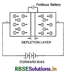
In forward biasing, the positive terminal of the battery is connected to p-type semiconductors and negative of the battery is connected to n-type semiconductors. As a result the holes of p-section and electrons in the n-section move towards the junction. If the applied voltage is sufficient to overcome the potential barrier of the junction, the two electrons and holes join together and these cease to exist as mobile charge carriers, For each electron hole pair, a covalent bond in p-region near the positive terminal of the battery breaks, and an electron is arrested by positive terminal and a hole is created, due to this breaking the hole moves towards the p-n junction. Similarly in the n-region, near the negative terminal of the battery more electrons arrive to replace the electrons lost due to combination with holes. This constant motion of electrons and holes produces a large current flowing through the junction.
Question 18.
Explain the flow of current in reverse biasing.
Answer:
In reverse biasing, the positive terminal of battery is connected to n-type semiconductors and negative of the battery is connected to p-type material of the p-n junction. As a result the holes in p-section and electrons in n-section move away from the junction with the result that the barrier layer is thickened leaving only a few thermally generated majority carriers to produce very small current. If we go on increasing the reverse bias, the temperature of p-n junction increases and this rise in temperature enhances the minority carrier concentration and the current increases rapidly. Beyond this limit, called zener voltage, the voltage across the junction remains constant for a large current.
Question 19.
What is depletion region? Explain the effect of forward bias and reverse bias on it.
Or
What is the cause of depletion layer in a p-n diode? What happens to the depletion layer width when p-n junction is forward and reverse biased?
Answer:
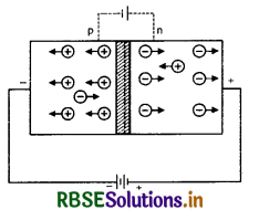
We know that in the n-type material electrons are the majority carriers and in the p-type material holes are the majority carriers. When a p-n junction is formed, due to this charged inhomogeneity some of the free electrons of the donor atoms on n-side will diffuse across the junction plane to the p-side where they fill valence levels created by the acceptor atoms. The net effect of the diffusion of the carriers across the junction is the creation on each side of the junction of a thin layer that is depleted (emptied) of mobile charge carriers (i.e. free electrons and holes). This is called depletion layer. Thus the diffusion of carriers across the junction is the cause of depletion layer. When p-n junction is forward biased, the width of depletion layer decreases and when it is reversed biased, the width of depletion layer increases.
Question 20.
Explain the need of doping a pure semiconductor.
Answer:
At 0 K a pure semiconductors has no free electron and behaves like an insulator, but at room temperature, some holes are created by thermal motion and number of holes are equal to number of electrons. The number of free electrons and holes can be increased by increasing the temperature of the semiconductors but it is of no practical importance because heat is dangerous enemy of semiconductors and bring complications to their functioning. The other method of increasing the conductivity of intrinsic semiconductors is by doping it with small amount of impurity.
Question 21.
Distinguish between forward biasing and reverse biasing in p-n junction. Discuss its use.
Answer:
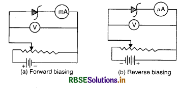
In a p-n junction, forward biasing is applied by connecting +ve of the battery to p-section and -ve of the battery to n-section. In the case of reverse biasing, +ve of the battery is connected to n-section and -ve of the battery is connected to p-section. As a result, the strength of the current
carriers moving in the circuit will change. It can be used by taking the arrangement to use it as half or full wave rectifier or in any other form. A graph between voltage and current for forward bias and reverse bias is as shown in the Fig. SAQ 21. From the fig., we find that during forward bias, the p-n junction offers less resistance and during reverse bias it offers large resistance.
Question 22.
What is the need of rectification?
Answer:
A number of electronic devices works only on d.c. Also for electrolysis, electrotyping, electroplating, anodising etc. direct current is needed. Hence we convert a.c. into d.c. Hence rectification is needed.
Question 23.
What is the difference between an ordinary p-n junction diode and a Zener diode?
Answer:
An ordinary p-n junction diode does not work on breakdown region whereas a Zener diode operates under reverse bias in breakdown region.
Question 24.
Which two machanisms are responsible for breakdown in p-n junction?
Answer:
(1) Avalanche breakdown. When reverse bias is increased, the minority carriers gain large kinetic energy and collide with the valence electrons of the atom and break the covalent bonds and pairs of electrons and holes are produced, the new carriers so produced generate additional carriers and a large number of free electrons and holes are produced. This cummulative phenomenon is called avalanche multiplication.
(2) Zener breakdown. This phenomenon is observed in those diodes that breakdown below about 6 V of reverse bias. At such a low voltage the depletion region is narrow of the order of 150-200 A, so there exists a high electric field of the order of 108 V m-1 across the junctions. This high electric field exerts a force on the bond electrons to tear them out of the covalent bond directly rather than by collision. Zener breakdown in thus a field emission phenomenon.
Question 25.
How can a zener diode be used to regulate the voltage?
Answer:
A zener diode is a specially designed p-n-diode which has a sharp breakdown voltage called zener voltage Vz. Hence zener diode can be used as a voltage regulator to keep the load voltage essentially constant at the value Vz, independent of variations in load current or supply voltage.
Question 26.
What is the effect of temperature on breakdown voltage in a p-n junction?
Answer:
If the reference voltage is above 6 V i.e. during avalanche multiplication temperature coefficient is positive and magnitude of avalanche breakdown voltage increases with increase in temperature. But below 6 V i.e. during zener breakdown, the temperature coefficient is negative and zener breakdown voltage decreases with an increase in temperature.
Question 27.
Why zener breakdown voltage decreases with increase in temperature?
Answer:
Because during avalanche breakdown, with the increase in temperature the amplitude of vibration of crystal atoms increases so the probability of collision of the carriers with crystal atoms increases, and there is loss of energy of the carriers and applied reverse voltage should be increased to make up the loss of energy to start avalanche process. But during zener breakdown, with the increase in temperature, the energy of valence electrons increases and it becomes easier for these electrons to escape from covalent bonds hence, zener breakdown voltage decreases with an increase in temperature.
Question 28.
What is a transistor?
Answer:
It is a semiconductor device in which a thin layer of one type Ge (or Si) is grown between two comparatively broad section of other type Ge (or Si) and is used to amplify impulses applied at its input terminal and can also act as oscillator.
Question 29.
How did the word transistor orginate?
Answer:
When emitter-base junction is forward biased and collector base junction is reverse biased, a low resistance of forward biased junction can be transformed into a high resistance of reverse biased junction. Also by interchanging biases, a high resistance can be transformed into a low resistance. Hence this junction trade is called transformer of resistor which in short becomes transistor.
Question 30.
Why do we prefer to use transistor amplifier in CE mode?
Answer:
In CE mode, the current gain and voltage gain are more than unity so this mode is used for current, voltage and power amplification. The input and the output resistances are intermediate between those for the CB and CC amplifier modes. This mode introduces a phase reversal between the input and the output voltages. Thus CE amplifier is most flexible and useful among the three modes.
Question 31.
Where do the electrons flow in a p-n-p transistor?
Answer:
The emitter of a transistor is always forward biased and the collector is always reverse biased. In p-n-p transistor the electrons in the base are repelled towards emitter-base junction by the forward voltage under the influence of electric field the electrons overcome the potential barrier and cross the emitter base junction, the electrons reaching into the emitter are minority carriers. The current which flows from base region to emitter region is due to the flow of electrons. This current is a function of emitter base potential. Since the width of base region is small, the ratio between the hole current and electron is very large and for practical purpose the electron current is neglected. Thus in p-n-p transistor, the holes are current carriers from emitter to collector, while the current conduction through the connecting wires of the external circuit is carried on by electrons.
Question 32.
Does the operating points of a transistor amplifier shift with temperature?
Answer:
Yes. Because the transistor parameter ß, is strongly dependent upon temperature no matter whether Ge or Si is used. Due to variation of transistor parameter ß, the collector current of a transistor changes rapidly and hence the operating point also shifts.
Question 33.
Define power gain of a transistor.
Answer:
The ratio of change of output power to the change in input power is called power gain
So power gain = \(\frac{\Delta P_{\text {out }}}{\Delta P_{\text {in }}}\)
Question 34.
Why CB configuration is seldom used?
Answer:
The basic function of transistor is to do amplification. But in CB configuration the current gain is less than unity in other words there is no gain in current. So for current gain we never use CB configuration.
Question 35.
List one application of CC configuration of a transistor.
Answer:
In CC configuration, the input and the output resistances are respectively the highest and lowest among the three modes. So CC configuration is used for matching a high impedance source to a low impedance load i.e. as a step down impedance transformer. It can also be used as a power amplifier since its current gain is large.
Question 36.
In a transistor base is made very thin. Why?
Answer:
A transistor consists of two semiconductors separated by a very thin base. This thin base is called depletion layer. It offers resistance to the motion of current carriers in the circuit. The resistance offered to those current carriers depends on the thickness of the base of the transistor. A thin transistor base will offer less resistance and this gives more current in the circuit.
Question 37.
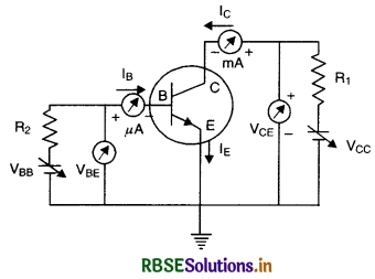
Draw a circuit diagram for use of NPN transistor as an amplifier in common emitter configuration. The input resistance of transistor is 1000 Ω. On changing its base current by 10 µA, the collector current is increased by 2mA. If the load resistance 5k Ω is used in the circuit, calculate the (i) current gain; (ii) voltage gain of amplifier.
Answer:
A transistor is a semiconductor device which is commonly used as a switch in electronic circuits and as an amplifier. It consists of three regions called Emitter, Base and Collector. The charge-carriers originate in the Emitter region and travel across the Base to the Collector region.
Here ∆Ib = 10 µA = 10 x 10-6 A
∆Ic = 2 mA = 2 x 10⁻³ A
Ri = 1000 Ω, RL = 5000 Ω
(i) Now ß = \(\frac{\Delta I_c}{\Delta I_b}=\frac{2 \times 10^{-3}}{10 \times 10^{-6}}\) = 200
(ii) AV = ß\(\frac{\mathrm{R}_{\mathrm{L}}}{\mathrm{R}_i}\) = 200 x \(\frac{5000}{1000}\)
or AV = 1000
Question 38.
Explain with the help of a circuit diagram, how the thickness of depletion layer in p-n junction diode changes when it is forward biased. In the following circuit, which one of the two diodes is forward biased and which one is reverse biased?
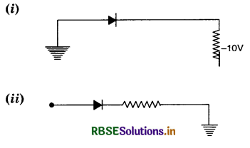
Answer:
When the p-n junction is forward biased, the majority carriers in each side (i.e. holes in p-section and electron in n-section) are pushed towards the junction. But the movement of electrons and holes across the junction is opposed by the fictitious battery voltage developed across the junction, hence the potential drop across the junction decreases and the diffusion of holes and electron across the junction increases. It makes the depletion layer thin and as such the junction diode offers very less resistance.
Here circuit (i) is reversed biased because p-section is at lesser potential (i.e. -10 V) as compared to n-section which is at a lower potential (i.e. -0 V).
Question 39.
A semiconductor has equal electron and hole concentration of 6 x 10⁸ m-3. On doping with certain impurity, electron concentration increases to 9 x 10¹² m-3.
(i) Identify the new semiconductor obtained after doping.
(ii) Calculate the new hole concentration.
Answer:
(i) Given ni = 6 x 10⁸ m-3
After doping with certain impurity, the electron concentration becomes ne = 9 x 10¹² m-3. Hence the doping is of pentavalent impurity and the new semiconductor is of n-type.
(ii) nh = ?
Since nehn = ni2
∴ nh = \(\frac{n_i^2}{n_e}=\frac{\left(6 \times 10^8\right)}{9 \times 10^2}\)
or nh = 4 x 10⁴ m-3.
Question 40.
Distinguish between an intrinsic semiconductor and p-type semiconductor. Give reason, why a p-type semiconductor crystal is electrically neutral, although nh >> ne?
Answer:
|
Intrinsic semiconductor |
P-type semiconductor |
|
1. It is natural semiconductor in pure form. |
1. It is a doped semiconductor with element from 3rd group. |
|
2. It has very small number of electrons and an equal number of holes. |
2. Number of holes is very large as compared to number of electrons. |
|
3. Current due to charge carriers is feeble (in µA). |
3. Current due to charge carriers is significant (in mA). |
The p-type semiconductor is electrically neutral because the excess holes get balanced by an equal number of electrons of the ionised wire in the lattice.
Question 41.
The figure SAQ 41 given below shows V-I characteristics of a semiconductor diode,
(i) Identify the semiconductor diode used.
(ii) Draw the circuit diagram to obtain the given characteristic of this device.
(iii) Briefly explain how this diode can be used as voltage regulator.
Answer:
(i) The semiconductor diode is a zener diode.
(ii) The circuit diagram to obtain the given characteristic is shown is Fig. SAQ 41 (a) and (b)
(iii) In a zener diode, the output is always constant even if the input voltage or load current varies. The zener diode is reversed biased to a fluctuating d.c. input voltage. Through a resistance R of suitable value, and the constant output voltage V0 is obtained across load. Resistance RL connected in parallel with the zener diode Fig. SAQ 41 (c).
Total current across R is the sum of Iz (across diode) and IL (across load)
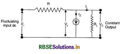
i.e. I = Iz + IL
And in a diode, V0 = Vz (always)
∴ Vi = IR + Vz
or Vi = IR + V0
or V0 = Vi - IR
So when Vi changes, I and hence IR changes in such a way that
V0 = Vz is constant.
On the other hand if Vi is constant and IL changes, then Iz changes in such a way that I (and hence IR) remain constant.
Thus in both the cases output voltage V0 remains constant.
Question 42.
The black box, shown here, converts the input voltage waveform into the output voltage waveforms as is shown in the figure SAQ 42.
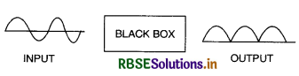
Draw the circuit diagram of the circuit in the ‘block box’ and give a brief description of its working.
Answer:
The black box has the circuit diagram of two diodes acting as a full wave rectifier as shown below:
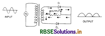
Working. During the positive half of input AC, D1 is forward biased and D2 reverse biased. Hence the current flows through the upper circuit as shown. During negative half, lower portion (D2) is forward biased and upper (D1) is reverse biased.
Thus during each half, we get the current either from D1 or from D2.
The output voltage is unidirectional having ripple contents.
Ripple factor of a rectifier = \(\frac{\text { r.m.s. of a.c. component }}{\text { value of d.c. component }}\)
To smoothen the output electric filters are used.The electric filters are combination of inductors are capacitors. Some of the useful filters are L-filter and π-filter.
Question 43.
Draw the (i) symbol and (ii) the reverse bias I-V characteristics of a zener diode. Explain briefly, which property of the characteristics enables us to use zener diode as voltage regulator.
Answer:
The symbol of zener diode is

Reverse bias I-V characteristics of zener diode is
Zener diode is a heavily doped p-n junction diode and is used in reverse bias. It can be operated in the breakdown region continuously (without being damaged) and the current is limited by external resistance, and the voltage drop across the zener diode is independent of the current flowing through it. This property of the zener diode enable us to use it as voltage stabilizer.
Question 44.
What is an intrinsic semiconductor? How can this material be converted into (i) p-type, (ii) n-type extrinsic semiconductor? Explain with the help of energy band diagrams.
Answer:
Intrinsic semiconductor. A pure semiconductor having no impurity in it is called as intrinsic semiconducter.
An intrinsic semiconductor doped by a suitable impurity is called an extrinsic semiconductor and is of two types:
(i) n-type semiconductor. When an intrinsic semiconductor say Si or Ge is doped by an impurity of an atom of + 5 valency element, we get a n-type semiconductor. This pentavalent impurity is called donor impurity (As, Sb, P etc.)
(ii) p-type semiconductor.When an intrinsic semiconductor say Si or Ge is doped by an impurity of an atom of +3 valency element, we get a p-type semiconductor. This trivalent impurity is called acceptor impurity (In, Al, B etc.).
Energy level diagrams:

Question 45.
In a transistor base is made very thin. Why?
Answer:
A transistor consists of two semiconductors separated by a very thin base. This thin base is called depletion layer. It offers resistance to the motion of current carriers in the circuit. The resistance offered to those current carriers depends on the thickness of the base of the transistor. A thin transistor base will offer less resistance and this gives more current in the circuit.
Question 46.
Draw a circuit diagram for use of NPN transistor as an amplifier in common emitter configuration. The input resistance of transistor is 1000 Ω. On changing its base current by 10 µA., the collector current is increased by 2mA. If the load resistance 5k Ω is used in the circuit, calculate the (i) current gain; (ii) voltage gain of amplifier.
Answer:
A transistor is a semiconductor device which is commonly used as a switch in electronic circuits and as an amplifier. It consists of three regions called Emitter, Base and Collector. The charge-carriers originate in the Emitter region and travel across the Base to the Collector region.
Here ∆Ib = 10 µA = 10 x 10-6 A
∆Ic = 2 mA = 2 x 10⁻³ A
Ri = 1000 Ω, RL = 5000 Ω
(i) Now ß = \(\frac{\Delta I_c}{\Delta I_b}=\frac{2 \times 10^{-3}}{10 \times 10^{-6}}\) = 200
(ii) AV = ß\(\frac{\mathrm{R}_{\mathrm{L}}}{\mathrm{R}_i}\) = 200 x \(\frac{5000}{1000}\)
or AV = 1000
Question 47.
Explain with the help of a circuit diagram, how the thickness of depletion layer in p-n junction diode changes when it is forward biased. In the following circuits, which one of the two diodes is forward biased and which one is reverse biased?
Answer:
When the p-n junction is forward biased, the majority carriers in each side (i.e. holes in p. section and electron in n-section) are pushed towards the junction. But the movement of electrons and holes across the junction is opposed by the fictitious battery voltage developed across the junction, hence the potential drop across the junction decreases and the diffusion of holes and electron across the junction increases. It makes the depletion layer thin and as such the junction diode offers very less resistance.

Here circuit (i) is reversed biased because p-section is at lesser potential (i.e. -10 V) as compared to n-section which is at a lower potential (i.e. -0 V).
Question 48.
A semiconductor has equal electron and hole concentration of 6 x 10⁸ m-3. On doping with certain impurity, electron concentration increases to 9 x 10¹² m-3.
(i) Identify the new semiconductor obtained after doping.
(ii) Calculate the new hole concentration.
Answer:
(i) Given ni = 6 x 10⁸ m-3
After doping with certain impurity, the electron concentration becomes ne = 9 x 10¹² m-3. Hence the doping is of pentavalent impurity and the new semiconductor is of n-type.
(ii) nh = ?
Since nehn = ni2
∴ nh = \(\frac{n_i^2}{n_e}=\frac{\left(6 \times 10^8\right)}{9 \times 10^2}\)
or nh = 4 x 10⁴ m-3.
Question 49.
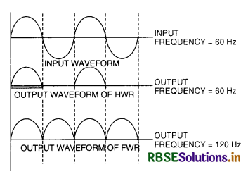
An ac input signal of frequency 60 Hz is rectified by a (i) half wave (ii) full wave rectifier. Draw the output waveform and write the output frequency in each case.
Answer:
Question 50.
Explain how the width of depletion layer in p-n junction diode changes when the junction is (i) forward biuased (ii) reverse biased.
Answer:
(i) Under forward biasing, the majority carriers in each side (i.e. holes in p-section and electrons in n-section) are pushed towards the junction. But the movement of electrons and holes across the junction is opposed by the potential barrier, hence the potential barrier across the junction decreases. It makes the depletion layer thin as shown in Fig. 50 (a).
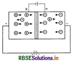
(ii) Under reverse biasing, the majority carriers in each side are pushed away from the junction. The movement of holes and electrons across the junction is supported by the potential barrier, hence the potential barrier across the junction increases. It makes the depletion layer thick as shown in Fig. SAQ 50 (b).
Question 51.
In a transistor, doping level in base is increased slightly. Now will it affect (i) collector current and (ii) base current?
Answer:
On increasing the deping level of base, its resistance increases, hence
(i) collector current decreases
(ii) base current increases.
Question 52.
Name the optoelectronic device used for detecting optical signals and mention the biasing in which it is operated. Draw its I-V characteristics.
Answer:
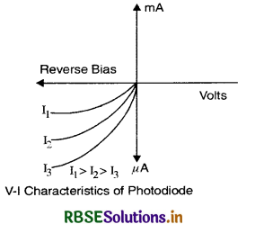
The name of the device is photodiode. It is operated in reverse bias I-V characteristic of photodiode is shown in fig. SAQ 52.
Question 53.
(a) In the following diagram, is the junction diode forward biased or reverse biased?
(b) Draw the circuit diagram of a full wave rectifier and state how it works.
Answer:
(a) Since p is at zero potential and n is at positive potential, so it is reversed biased.
(b) Full wave rectifier: The circuit of the full wave rectifier can be constructed in two ways. The first method uses a centre tapped transformer and two diodes. This arrangement is known as a centre tapped full wave rectifier. The second method uses a standard transformer with four diodes arranged as a bridge. This is known as a bridge rectifier. In the next section, we will restrict the discussion to the centre tapped full wave rectifier only. You can read our article on bridge rectifier to learn the construction and working of bridge rectifier in detail.
Question 54.
Explain the two processes involved in the formation of a p-n junction diode. Hence define the term “barrier potential.”
Answer:
The two processes involved are diffusion and drift.
Diffusion: It is the process of movement of majority charge carriers i.e. holes from p-region into n-region and electrons from n-region across the junction due to different concentration gradient on both sides of the junction.
Drift: It is the process of movement of minority carriers i.e. holes from n-region and electrons from p-region due to the development of electric field at the junction.
Barrier potential: Due to migration of holes and electrons, the two sections of the junction diode no longer remain neutrals and a potential difference across the junction is developed. The potential difference is such that it opposes and then stop the further flow of charge carriers. This potential is called potential barrier (or barrier potential).
Question 55.
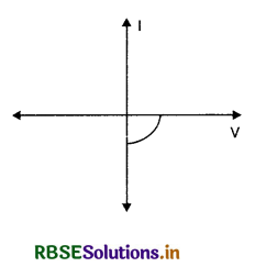
Name the junction whose I-V characteristics are shown below.
Answer:
This is the I-V characteristics of solar cell.
Question 56.
(i) Describe briefly the functions of the three segments of n-p-n transistor.
(ii) Draw the circuit arrangement for studying the output characteristics of n-p-n transistor in CE configuration. Explain how the output characteristics is obtained.
Answer:
(i) (a) Emitter: Supplies the large number of majority carriers for current flow through the transistor.
(b) Base: Allows most of the majority charge carriers to go over to the collector.
(c) Collector: Collects a major portion of the majority charge carriers supplied by the emitter.
(ii) The circuit arrangement is as shown.
The output characteristics are obtained by observing the variation of Ic when VCE is varied keeping IB constant.
Long Answer Type Questions
Question 1.
Explain the formation of energy bands in solids and hence define conduction band and valence band.
Or
What are energy bands? Explain the formation of energy bands in case of silicon crystal.
Answer:
In an atom, the electrons revolve around the nucleus in almost circular orbits (Bohr’s model). Energy of electrons in each subshell is definite. These definite energy values are called energy levels of the atoms. But in crystals, atoms are arranged in a regular and periodic manner. A solid crystal contains about 1023 atoms/cm3. So each atom is in the electrostatic field of neighbouring atoms and due to interaction between the atom, the modification of energy level takes place. The maximum effect of the interaction is on the valence electron and the energy E between E + ∆E. Thus each energy level becomes broad. This broadening of energy level is called energy band. The electrons in the inner shell are strongly bound to the nuclei, so they are slightly affected by the presence of neighbouring atoms. They are called core levels. If an energy bond consists of as much electrons as permitted by Pauli’s Exclusion Principle, then it is said to be completely filled band, and in such a band there will be no free electrons for conduction of electricity, while for a partially filled band conduction is possible.

In order to understand how the modification of energy level takes place, let us consider a single crystal of Si having N atoms. The electronic configuration of Si is 1s2, 2s2, 2p6, 3s2, 3p2. The energy levels of Si atom in isolated state as well as in the crystal form are shown in Fig. 14.85. Here the interatomic spacing is r and distance ‘a’ corresponds to the crystal lattice spacing. The process of splitting is summarised as follows:
1. When r > c.
The atomic spacing is sufficiently wide, so the interaction between atoms is negligible and practically, here is no modification of 3s and 3p energy sublevels.
2. When r = c.
When atoms are brought further close to each other, their interaction increases and the real splitting of the sublevels starts. The energy difference between 3s and 3p sublevels is denoted by double arrow and is called forbidden gap.
3. When r < c.
The forbidden gap decreases and reduces to zero at r = b2. So at r = b2 the two bands overlap. At a distance between b2 and c instead of single 3s or 3p level, we get a large number of closely packed levels. The number N is very large so this collection of closely spaced levels is called an energy band.
4. When b1 < r < b2.
When the atomic spacing is further reduced, the 3s and 3p levels remain merged into each other and thus there is no restriction on the electrons to move from 3s sublevels to 3p sublevel or vice versa. The energy gap between 3s and 3p disappears, and the two band overlap. In this situation all 8N levels (2 from s and 6 from p) are now continuously distributed. Here we cannot distinguish between the electrons belonging to 3s and 3p sublevels. At such a situation one can only say that 4N sublevels are filled and 4N sublevels are empty.
5. When r = a.
This is known as equilibrium distance because the atoms in crystal lie at this interatomic separation. Here is the band divide and spread widely Here we find that band of filled energy level and empty energy level are separated by an energy gap called forbidden gap or forbidden band. The lower band which is completely filled up is known as valence band and the upper band which is normally (at 0 K) empty, is referred to as the conduction band.
The gap between valence band and conduction band is called fobidden band and it is a measure of energy E. Thus E is the amount of energy that should be given to the electron in valence band, so that it could jump to the conduction band. For insulator it is of the order of 5 to 10 eV, and for semiconductor like Ge is about 0.72 eV and for Si it is about 1 eV.
Question 2.
On the basis of the enrgy band diagrams distinguish between metals, insulators and semiconductors.
Answer:
In insulator. In insulators, valence band is completely filled and conduction band is completely empty. The energy gap (Eg) between the two is so large that the electrons cannot overcome it and, hence, conduction is not possible. Therefore, insulators are poor conductors of electricity. Electrons cannot gain energy from the applied field and current cannot flow. An important example of insulator is diamond with energy gap of about 5.4 eV (Fig. LAQ 2 (a))

Semiconductors
The energy and structure of a semi conductor is shown in Fig. LAQ 2 (b) It is similar to that of an insulator but with a comparatively small energy gap of about 1 eV. At absolute zero of temperature, the conduction band of semiconductor is totally empty, and all the energy states in the valence band are filled. The absence of electrons in the conduction band at absolute zero does not allow current to flow under the influence of an electric field. Therefore, they are insulators at low temperatures.
However, at room temperature, some valence electrons acquire thermal energy greater than the energy gap Eg and move to the conduction band where they are free to move under the influence of even a small electric field. Common examples of semiconductors are silicon (14), Germanium (32) with energy gap of about (1.12 eV) and 0.75 eV respectively. The gap (band) that separates conduction and valence band is called Forbidden Band.
Metals (Conductors)
The energy band structure of a metal is shown schematically in Fig. LAQ 2 (c). The last occupied band of energy levels is only partially filled:
The available electrons occupy, one by one (Pauli exclusion principle) the lowest levels. This leaves part of the band (called conduction band unoccupied.
The highest energy level occupied at absolute zero by electrons is partially filled conduction band, is called Fermi level and the corresponding energy is called Fermi energy.
When an electric field is applied, electrons gain energy (about 108 eV). They can be excited to empty energy levels immediately about the Fermi level and some of the electrons are accelerated in the direction of the field. Thus electric current is conducted through the conductors.
Question 3.
(a) Explain formation of holes in a semiconductor.
(b) What are intrinsic semi-conductors?
Answer:
(a) Hole At 0 K, semiconductor is an insulator. As the temperature increases electrons in a semiconductors move to conduction band. In the valence band, a valence is created at the place where electron was present before moving to the conduction band. This vacancy is called hole.
Another Explanation
Consider a Germanium crystal. In it the atoms are strongly held by covalent bonds. On receiving an additional energy, one of the electrons contributing to a covalent bond breaks and is free to move in the crystal lattice. While coming out of the covalent bond, it leaves behind a hole which is shown as an open circle. An electron from a neighbouring atom can break away and can come to the place of the missing electron (or hole) completing the covalent bond and creating a hole at another place.
The breaking of bonds or generation of electron-hole pairs, and completion of bonds due to recombination is taking place all the time. At equilibrium, the rates of generation becomes equal to the rate of combination, giving a fixed number of free electrons and holes.
(b) Intrinsic semiconductors. A semi-conductor, which is quite pure and completely free from any impurity is called an intrinsic semiconductor. Silicon and germanium are two important examples of intrinsic semiconductors.
In Si or Ge each of the four valency electrons enter into a covalent bond with one valency electron each of the four neighbouring atoms. By forming such covalent bond, the atoms behave as if their outermost orbits are complete with eight electrons, leaving no free electrons. The valency electrons now occupy filled energy bands. There is some energy gap between the filled valence band and the conduction band. Even at room temperature, the thermal energy imparted to the valence band is enough to enable some electrons to break away from the covalent bond and enter into the conduction band leaving behind equal number of vacant sites near the top of valence band. These vacant sides are called holes.
These electrons in the conduction band start drifting under the applied electric field and are responsible for the moderate electric conductivity of semiconductors. The electric conductivity of pure semiconductor is called intrinsic conductivity.
In intrinsic semiconductors
ne = nh = ni, .......................(1)
where ne is the electron density in conduction band. nh is the hole density in valence band and ni is intrinsic carrier concentration.
Question 4.
(a) What is an extrinsic semiconductor?
(b) What are n-type and p-type semiconductors?
Answer:
(a) Extrinsic semiconductors
A doped semiconductor or a semiconductor with impurity atoms is called an extrinsic semiconductor.
n-Type semiconductor.
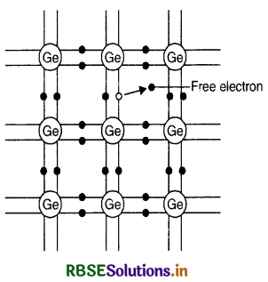
The conductivity of intrinsic semiconductor is zero at absolute zero and very small at ordinary temperatures. Germanium has 4.52 x 10²² atoms per cm3. An addition of only one impurity atom per million Ge atom, is sufficient to give desired conductivity to it. The process of deliberately adding suitable impurity atom to the intrinsic semiconductor is called Doping (the impure semiconductor is called a doped semiconductor). If we dope intrinsic Ge. with a controlled amount of pentavalent atoms, say antimony Sb or phosphorus P, which has five valence electrons, the atoms of the impurity element will substitute the Germanium atoms (Fig. 14.89(a)). Four of the five valence electrons is comparatively free to move. The pentavalent atoms are called the donor atoms because they donate electrons to the host crystal extrinsic semi-conductor are called n-type. On giving up their fifth electron, the donor atoms become positively charged. However, the material remains electrically neutral as a whole.

The extra electron of the donor atom orbits around the donor nucleus.
Explanation on the basis of band. In the band language, we would say that this electron, free to move about, has the lowest possible energy in the empty conduction band. Thus, the energy level diagram of a doped n-type semi-conductor is as shown in the [Fig. LAQ 4 (b)] For phosphorus or arsenic in silicon, the lowest donor electron energy level lies below the bottom of the conduction band. This energy is comparable to room temperature. Thermal energy is much smaller than the energy gap Eg = 1.1 eV
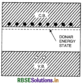
Since, it requires less energy to free a donor electron (or ionize the donor atom) than to promote an electron from the valence band to the conduction band, at any non-zero temperature, a sizeable fraction of the donor electrons is in the conduction band. In n-type electron density is greater than hole density ne > nh.
p-Type semiconductors
In p-type Ge. If we dope intrinsic Ge, with a controlled amount of trivalent atoms, say indium (In or boron B or aluminium Al) Group III, which has three valence electrons, impurity atom will occupy places of some Ge atoms and there will be one incomplete covalent bond with a neighbouring Ge atom, due to the deficiency of an electron. This is completed by taking an electron from one of the Ge-Ge bonds, thus completing the In-Ge bond. This makes In ionized (negatively charged), and creates a ‘hole’ or an electron deficiency in Ge.
The trivalent atoms are called acceptor atoms and this extrinsic semiconductor is known as p-type.

Explanation on the basis of band theory
In a p-type semiconductor at room temperature, the holes are free to move about in the valence band because the acceptor atoms are nearly all ionized due to thermal energy.
Therefore, the hole density in valence band is equal to the acceptor density Na. In p-type semiconductor the hole density is greater than the electron density,
i.e. Na = nh >> ne.
Question 5.
(a) Define a hole. What are its characteristics?
(b) Explain that energy of a hole is high.
Answer:
(b) Hole. The absence of electrons from a certain set of filled electrons states is often conveniently described in terms of holes.
Properties of Hole
- Hole carries a positive charge.
- Mass of hole is the same as that of electron.
- It is an absence of electron.
- Energy of hole is higher, the farther below it is from the top of the valence band.
(b) Energy of hole is high. To see this, imagine an electron being removed from the filled valence band to the bottom of the empty conduction band. This removal creates a hole in the valence band. Clearly it requires more energy to remove an electron which is farther from the top of the valence band. Thus a valence hole state farther from the top of the valence band has higher energy, just a conduction electron farther from the bottom of the conduction band has higher energy.
Question 6.
Discuss the current conduction in n-type and p-type semiconductors.
Answer:
Current conduction in semiconductors
In a semiconductor the charge carriers are electrons in the conduction band and holes in the valence band. They move randomly in all directions owing to the fact that their thermal energy and net current in any direction is zero. When an external electric field is applied, every charge carrier experiences a force and drifts in the direction of the force. In the steady state, the rate of momentum gained from the field equals the rate of loss of momentum due to scattering. A steady drift velocity is thus achieved giving rise to a steady flow of current.
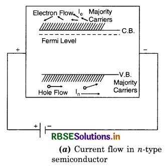
In n-type semiconductor
In an n-type semiconductor concentration of minority charge carriers, i.e. holes, is negligible in comparison with the concentration of majority charge carriers i.e. electrons. When potential difference is applied across the n-type semiconductor [Fig. LAQ 6 (a)], the free electrons (donated by impurity) in the crystal will be directed towards the positive terminal. On reaching the positive terminal the electrons disappear and the immobile positive ions in the vicinity of the negative terminal remain unneutralized. These ions immediately attract electrons from the negative terminal. Thus a continuous flow of electrons from one terminal to the other terminal via the semiconductor takes place.
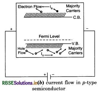
In p-type semiconductor
In a p-type semiconductor, concentration of minority carriers i.e. electrons is negligible in comparison with the concentration of majority charge carriers t.e.holes. When potential difference is applied across the p-type semiconductor, the holes (donated by the impurity) shifted from one covalent bond to another. As the holes are positively charged, so they are directed towards the negative terminal [Fig. LAQ 6 (b)]. On reaching the negative terminal they combine with electrons coming out of negative electrode and disappear because as the holes drift away from the positive terminal they leave behind the unneutralized immobile negative charges. These charges and the positive electrode give rise to an electric field which cause the ionizing electrons to leave the acceptor atom and come to the positive electrode where they are lost. By losing an electron in the above process the acceptor atom attempts to steal an electron from the adjacent bond. A hole is thus formed. Thus the current in p-type semiconductor is due to the motion of the holes whereas in the external circuit it is due to the motion of electrons. It may be noted that in p-type conductivity, the valence electrons move from one covalent bond to another unlike the n-type where current conduction is by free electrons in the conduction band.
Question 7.
Derive an expression for the conductivity of a semiconductor.
Or
Show that resistivity of semiconductor depends upon their densities and their mobilities.
Or
Explain why the conductivity of intrinsic semiconductor increases with rise in temperature.
Answer:
Consider a block of a semiconductor of length l and area of cross-section A. Let an electric field E be applied across its ends and a potential difference V is acting across its ends as shown in figure 14.91. The electrons and holes in the semiconductor are moving due to this applied electric field. Both electrons and holes contribute to the current. The total current I can be written as the sum of the contribution of electron and hole currents.
∴ I = Ie + Ih
Where Ie = current due to electrons, and Ih = current due to holes. Both electrons in the conduction band and holes in valence band are moving randomly as electrons in a metal.
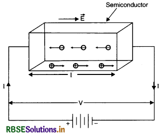
But using the relation
Ie = ne Ave e, and for the hole
Ih = nh Avh e, we get
I = neAeVe + nhA Vhe
Where ne is the magnitude of the electron charge, n is the electron density and nh is hole density and ve and vh are electron and hole drift velocities. A low applied electric fields, semiconductors obey Ohm’s law so that
I = \(\frac{\mathrm{V}}{\mathrm{R}}\) = eA (ne ve + nh vh)
But V = El,
\(\frac{\mathrm{E} l}{\mathrm{RA}}\) = e(ne ve + nh vh)
But ρ = \(\frac{\mathrm{RA}}{l}\) (∴ R = ρ\(\frac{1}{\mathrm{~A}}\))
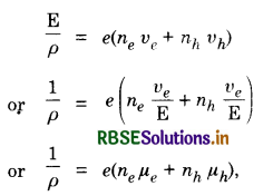
where µe and µh is the mobility of electrons and holes respectively (the mobility µ is defined as the drift velocity per unit electric field).
The conductivity σ\(\left(=\frac{1}{\rho}\right)\) given by
σ = \(\frac{1}{\rho}\) = e(ne ve + nh vh) .................(i)
The eq. (i) shows that the resistivity of a semiconductor depends on the electron and hole densities and their mobilities. With the increase of temperature of the semiconductor, the value of ne and nh also increases. Hence the conductivity a of semiconductor increases with the increase in temperature.
Question 8.
What is p-n junction? What is the method of developing a p-n junction?
Answer:
P-N Junction. When p-types and n-type semiconductors are brought into contact, the resulting arrangement is called p-n junction. Due to high concentration of free electrons in n-type crystals, some free electrons diffuse through the junction to the p-region. Similarly some holes from p-region diffuse to n-region.
A p-type or n-type silicon or Ge crystal can be grown by adding appropriate impurity in the metal. These crystals are cut into thin slices called the wafer. Semiconductor devices are usually made on these wafers. If on a wafer of n-type silicon, an aluminium film is placed and heated to high temperature, Say 580°C, aluminium diffuses into silicon. In this way a p-type semiconductor is formed on an n-type semiconductor. Such a formation of p-region on n- region is called the p-n junction.
Question 9.
Discuss p-n junction as a diode.
Answer:
Formation of junction diode. When a p-type crystal is placed in contact with n-type crystal so as to form one piece, the assembly so obtained is called p-n junction or junction diode or crystal diode. The surface of contact of p-type and n-type crystals is called junction. In the p-section, holes are the majority carriers while in n- section, the electrons are majority carriers. Due to the high concentration of different types of charge carriers in the two sections, holes from p-region diffuse into n-region and electrons from n-region diffuse into p-region. In both cases, when an electron meets a hole, they cancel the effect of each other and as a result, a thin layer at the junction becomes devoid of charge carriers.This is called depletion layer as shown in the figure LAQ 9. The thickness of depletion layer is of the order of 10-6 m.
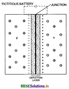
Due to the migration of holes and electrons, the two sections of the junction diode no longer remain neutral. The p-section of the junction diode becomes slightly negative, while the n-section is rendered positive. Due to this, there is a potential gradient in the depletion layer, negative on the p-side and positive on the rc-side. In other words, it appears as if some fictitious battery is connected across the junction with its negative pole connected to p-region and positive pole connected to n-region. The potential difference developed across the junction diode due to migration of majority carriers is called potential barrier. The magnitude of the potential barrier is about 0.3 V for Ge junction diode and about 0.V for Si junction diode. Further, the value of potential barrier depends on the amount of doping of the semiconductor crystal.
It may be pointed out that across the junction, a very large electric field is set up due to potential difference developed across it.
E = V = \(\frac{0.7}{10^{-6}}\) = 7 x 10⁵ Vm-1
The symbol of p-n junction diode is

The direction of arrow is from p to n. p is called anode and n is called cathode.
Question 10.
Explain briefly, with help of circuit diagram, how V-I characteristics of a p-n junction diode are obtained in (i) forward bias, and (ii) reverse bias. Draw the shape of the curves obtained.
Or
Discuss the variation of current with voltage in a p-n junction diode when it is forward biased.
Answer:
Methods of basing. There are two methods of biasing p-n junction.
(i) Forward biasing. A p-n junction is forward biased when the positive terminal of the external voltage source is connected to its p-side and the negative terminal to its n-side. The positive and negative voltages of the battery repel the holes and electrons (i.e majority carriers) towards the junction simultaneously as shown Fig. LAQ 10 (a).
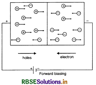
(ii) Reverse biasing. A p-n junction is said to be reverse biased when the positive terminal of the external voltage source is connected to its n-side and the positive terminal is to its p-side. The positive and negative of the battery attract the holes and electrons (i.e. majority carrier) towards the ends of p-n junction simultaneously as shown in Fig. LAQ 10 (b)
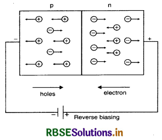
Circuit Symbols
When the diode is forward biased, the tail of the arrow (or anode) is connected to the positive terminal of the battery, figure LAQ 10 (c) and wshen the diode is reversed biased, the head of the arrow (or cathode) is connected to the positive terminal, figure LAQ 10 (d).
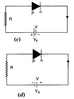
Current in forward biased diode. Initially when forward bias voltage is zero, current is also zero. When p-n junction is forward biased, the positive holes in the p-type material are repelled by the positive voltage towards the junction. Simultaneously the free electrons in the p-type material are repelled by the negative voltage towards the junction (a minimum voltage of 0.7 V for Si and 0.3 V for Ge is needed to overcome the potential barrier at the junction) Fig. LAQ 10 (a). Practically no current flows until the barrier is overcome.
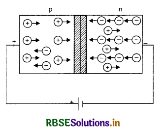
Initially when forward bias voltage is zero, current is also zero. As bias voltage is increased, little by little current remains zero till bias voltage is 0.3V (potential barrier). When bias voltage increases, from potential barrier current starts flowing and the thickness of depletion. Increasing bias voltage further makes more and more free charge carriers to move towards junction, thus increasing current. With forward voltage of about 2 volts, the covalent bonds between atoms break, setting more electrons and holes free in each section. Their movement increases the current suddenly. Forward bias voltage is not increased beyond 3V to prevent rupturing (break down). Forward bias characteristic is as shown in Fig. LAQ 10 (f)
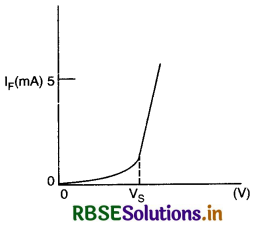
The curve is almost linear. The voltage at which the current starts to increase rapidly is called the cut in or knee voltage of the diode (It is about 0.3 V for Ge and about 0.7 V for Si)
Current in Reverse Biased Diode When the p-region is connected to negative terminal and n-region to the positive terminal of the battery, the diode is said to be reverse biased. The holes are now attracted towards the negative of battery from the p-region and move away from the junction. The electrons also get attracted by the positive terminal and move away from the junction. [Fig. LAQ 10 (g)].
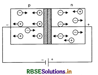
As a very small number of holes and electrons are left in the vicinity of the junction, flow of current almost stops completely. A small current of a few milliamperes still flows due to minority carriers. Some covalent bonds always break down because of the normal heat energy of the crystal molecules. Electrons liberated by this process in the p-region move to the left across the junction, while holes generated in the n-region by heat move to the right under the electric field applied by the battery. Thus, a small electron hole combination current is maintained by these so called minority carriers. If the reverse bias is made very high, the covalent bonds near the junction break down and a large number of electron-hole pairs are liberated and the reverse current increases abruptly to a relatively high value. The maximum reverse p.d. which a diode can tolerate without break down is called reverse break down voltage or zener voltage. It is greater for Si than for the Ge. The graph between p.d. and current in the reverse bias is as shown in Fig. LAQ 10 (h)
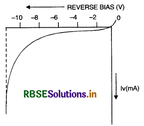
Question 11.
(a) What is rectification?
(b) How does p-n junction act as
(i) half wave rectifier
(ii) full wave rectifier?
Answer:
(i) p-n junction as half wave rectifier principle
It is based on the principle that in a p-n junction diode the current flows only if it is forward biased and negligible current flows if it is reverse biased.

(b) (1) Circuit arrangement
The basic circuit for half wave rectifier is as shown in Fig. LAQ 11 (a). Most electronic equipments have a transformer at the input. The transformer allows us to step the voltage up or down to get desired level of d.c. voltage and can provide isolation from the power line and thus reduces the risk of electrical shock. The a.c. supply to be rectified is applied to the primary (P) of a transformer. The secondary (S) is connected in series with the diode and the load resistance RL. The d.c. output is obtained across the load Rl. Since diode conducts only for half cycle of the a.c. voltage applied (i.e. when forward biased), and does not conduct for the negative half cycle, thus in this case it is known as half wave rectifier.
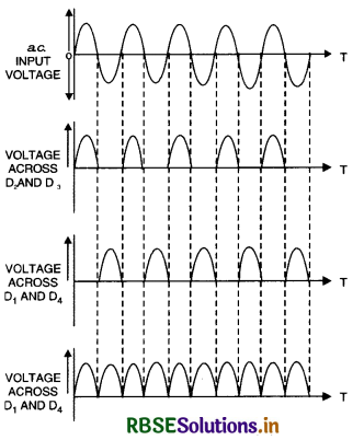
Theory
During positive half of input a.c., the point A is positive and B is negative. The diode D2 and D3 are forward biased and conduct, while D1 and D4 are reverse biased and do not conduct. These two diodes are in series through the load RL and the direction of conventional current is shown by full arrows.
(ii) Peak inverse voltage is shared by one diode. So this rectifier cannot be used for high voltages.
(ii) Bridge Rectifier
Bridge rectifier is the most widely used of all the rectifiers. It is a full wave rectifier and does not require centre tapped transformer.
Circuit arrangement
It consists of four diodes D1, D2, D3, and D4 which are connected to form a bridge as shown in Fig. LAQ 11 (e). The a.c. supply to be rectified is applied to the diagonally opposite ends of the bridge through the transformer and the load resistance RL is connected between the other two ends of the bridge.

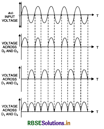
During negative half of input o.c., the point B is positive and A is negative. The diodes D1 and D4 are forward biased and conduct while D2 and D3 are reverse biased and do not conduct. These two diodes are in series through the load RL and the direction of conventional current is shown by dotted arrows. We find that whether diodes D2 and D3 conduct or D4 and D4 conduct, the direction of current in both the half cycles along the load RL is always from D to C. The waveform of input and output voltage is as shown in Fig. LAQ 11 (f).
Advantages
- Centre tapped transformer is not required.
- The full voltage of secondary is applied across the two conducting diodes. So the output is twice that of the centre tap circuit for the same secondary voltage.
- Peak inverse voltage is half that of conventional centre tap rectifier.
Disadvantages
- It is un-economical as it requires four diodes.
- Since during each half cycle of a.c. input two diodes that conduct are in series. So voltage drop across the internal resistance of the diodes is double of the value in the centre tap circuit and thus the efficiency of the bridge rectifier is very low.
Question 12.
What do you mean by light emitting diodes? Why are they so called? State applications of LEDs. Why we prefer LEDs over conventional incandescent lamps?
Answer:
Light emitting diodes
A light emitting diode (LED) is a specially made p-n junction diode (gallium arsenide phosphide (GaAsP) in which when current is made to flow in the forward direction, visible light is emitted from the region of the depletion layer. We know that, on forward biasing a p-n junction, the potential barrier gets lowered and the majority carriers start crossing the junction. The conduction band electrons from the n-region cross the barrier and enter the p-region. Immediately on entering the p-region each electron falls into hole and recombination takes place. Also some holes may cross the junction from p-region to n-region. A conduction band electron in the n-region may fall into a hole even before it crosses the junction. In either case, recombination takes place around the junction. Each recombination radiates energy in a visible form. Such a light emitting diode is referred to as an LED for short. Photons with energy hv = Eg are emitted. The corresponding emission wavelength is given by
λ = \(\frac{h c}{\mathrm{E}_{\mathrm{g}}}\),
where h is Planck’s constant (h = 6.62 x 10⁻³⁴ Js), c is the velocity of light (c = 3 x 10⁸ ms-1) and in case of GaAsP band gap Eg = 1.90 eV, the above expression gives
λ = \(\frac{6.62 \times 10^{-34} \times 3 \times 10^8}{1.90 \times 1.6 \times 10^{-19}}\)
= 6500 Å
which corresponds to visible light. A manufacturer by a proper choice of band gap and material can produce LEDs that radiate red, green or orange fights. Infrared LEDs use gallium arsenide (GaAs), which emits invisible radiations and can be used in burglar alarm system and other areas requiring invisible radiation.
Applications
- The infrared LEDs can be used in burglar alarm system and other areas requiring invisible radiations.
- They are used in instrumental displays, panel indicators, digital watches, calculators, multimeters, intercoms, telephone switch boards etc.
- They are rapidly replacing cathode ray tubes in solid state video displays.
Advantages over incandescent light sources
- They consume less power as they work on low voltage (1 to 2V) and currents (5 to 10 mA).
- They are not affected by mechanical vibrations.
- They have long life, even more than 20 years.
- They require no heating, no warm up time, and hence are very fast in action, since, unlike an incandescent lamp, they can be switched on or off in 1 sec.
Question 13.
Explain the principle, construction and working and uses of a photo diode.
Answer:
Photo diode
A photo diode is a p-n junction having photosensitive semiconducting material.
Principle. It is based on the principle of electric conduction from light.
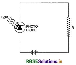
Construction and working
A photo diode is a p-n junction made from photo¬sensitive semiconducting material. In a reversed biased p-n junction, when fight is made to fall, the valence band electrons absorb this energy and jumps to conduction band leaving a hole in the valence band, so additional electron hole pairs are created in both p and n regions Fig LAQ 13. In this process , a small change in majority carrier concentration and a large change in minority carrier concentration take place. Thus the reverse current increased to a large value due to additional minority carriers. As the intensity of incident light is increased, the current increases almost linearly till it becomes maximum. The maximum current is called saturation current.
Uses.
- Photo diodes are used as photo-detectors to detect the radiations.
- They are used in light operated switches.
- They are used in sound films, reading of computer punched cards and tapes etc.
Question 14.
Explain the principle, construction and uses of a solar cell.
Answer:
It is a p-n junction which converts light energy into electric energy.
Principle. It is based on the principle of production of potential difference by sun light.
Construction
A solar cell is a p-n junction diode which converts sun light directly into electric current. In a solar cell having p-n junction, either p or n section is made very thin so that the light energy falling on the diode is not greatly absorbed before reaching the junction. The thin region is called emitter and the other region is called the base.
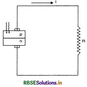
Working
When light is made to fall on the solar cell, photons of light are absorbed and electron-hole pairs are created in both p and n regions which are separated by a strong barrier field across the depletion layer. The hole in n-side move towards the p-side, similarly electrons in p-side move towards n-side and in an open circuit, the accumulation of electrons and holes on two sides gives rise to open circuit voltage. If a load resistance is connected across the p-n junction, the current flows in the circuit (Fig. LAQ 15). The maximum current is called the short-circuit current. The magnitude of the current is proportional to the light intensity.
Uses.
- Solar cells are used to charge batteries in day time and then use them during night as a source of electrical energy.
- They are used in satellites and space vehicles to provide power supply.
- They are used in street fights, solar geysers etc.
Question 15.
What is a zener diode? Describe the physical mechanism for zener breakdown. What are the uses of a zener diode?
Answer:
The Zener diode
A specially designed p-n junction diode which has a sharp breakdown voltage is called a zener diode. The current that flows under reverse breakdown is not necessarily destructive if the amount is limited to a value such that the diode does not become overheated. By suitably controlling the amount of impurity and making the p-n junction free from surface imperfections, the voltage at which breakdown takes place can be made to occur very distinctly and sharply, as shown in Fig. LAQ 15. This type of diode is called a
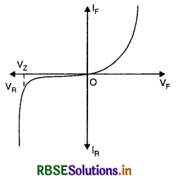
zener diode and the breakdown voltage Vz is called Zener Voltage.
Zener voltage depends upon the amount of doping. If the diode is lightly doped the breakdown voltage has higher value and if it is heavily doped, the breakdown voltage will occur at a lower value.
The following points may be noted about he zener diode.
- A zener diode is always reverse biased.
- A zener diode has sharp breakdown voltage called zener voltage Vz.
- A zener diode is like a conventional diode except that it is properly doped to have a sharp breakdown voltage.
- In forward bias-conditions, a zener diode acts like a conventional p-n junction diode.
- The zener diode is not immediately burnt simply because it has entered the breakdown region. As long as the external circuit connected to the diode limits the diode current to less than burnt out value, the diode will not burn out.
6. Temperature Coefficient
The temperature coefficient is defined as the percentage change in reference voltage per degree Celsius change in diode temperature. These data are supplied by the manufacturer. The coefficient may be either positive or negative and will normally be in the range ±0.1 per cent/°C. If the reference voltage is above 6 V, where the physical mechanism involved is avalanche multiplication, the temperature coefficient is positive. However, below 6V, where true zener-breakdown is involved, the temperature coefficient is negative.
Uses.
Zener diodes find numerous applications in transister circuitry. Most important of them are:
- as voltage regulators.
- as a fixed reference voltage in a network for biasing and comparison.
- for calibrating voltmeters.
- for avoiding meter damage by accidental application of excessive voltage.
Question 16.
Discuss a zener diode as voltage stabiliser.
Answer:
Zener diode as voltage stabiliser
It is desired in many electronic applications that the output voltage should remain constant inspite of variations in the input or load. In order to ensure this, a voltage stabilising device called voltage stabiliser is used. There are many stabilising circuits, let us discuss only one such circuit i.e. zener diode as voltage stabiliser.
Construction. The basic Zener diode d.c. voltage regulatory circuit is shown in Fig. LAQ 16. It consists of a resistance RS connected in series with the input voltage, and a zener diode connected in parallel with the load resistance RL across which a constant output voltage is desired. The Zener diode is reverse biased with the input voltage whose variations are to be regulated. The resistance RS absorbs the output voltage fluctuations so as to maintain constant voltage across the load. The diode is selected with a zener breakdown voltage Vz equal to the voltage desired across the load. The zener diode acts as a bypass valve, through which more current can pass when an increase in input volta'ge or a decrease in load current occurs, maintaining the voltage at the output nearly constant at Vz.
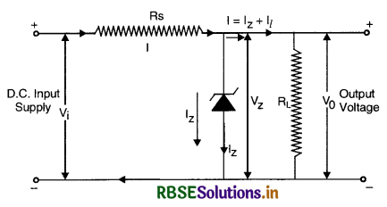
Working. If the reverse voltage across a Zener diode is increased beyond the breakdown voltage Vz, the current increases sharply and large current I2 flows through the zener diode and the voltage drop across Rs increases maintaining the voltage drop across RL at constant value V0 = Vz.
On the other hand, if we keep input voltage constant and decrease the load resistance RL, the current across the load will increase. The extra current cannot come from the source because drop in Rs will not change as the zener is within its regulating range. The additional load current will come from a decrease in zener current Iz so that the total current (Il + Iz) remains constant. Consequently, the output voltage remains at constant value.
Let I = Current from the source.
Iz = Current through Zener diode.
Voltage drop across Rs,
Vs = Input voltage - Vz
or IRs = Vi - V0
Current through Rs
I = Iz + Il
Applying Ohm’s law, we have
Rs = \(\frac{\mathrm{V}_i-\mathrm{V}_0}{\mathrm{I}_z+\mathrm{I}_{\mathrm{L}}}\)
d.c. resistance of zener diode = \(\frac{\mathrm{V}_0}{\mathrm{I}_z}\)
Question 17.
What do you mean by a junction transistor? What are their types and give their symbols?
Answer:
Junction Transistor
It is an arrangement obtained by growing a narrow of either n-type crystal between two relatively wide sections of p-type or by growing p-type by crystal between two relatively wide sections of n-type crystals.
Junction transistor is of two type:
(i) In which a narrow layer of n-type semiconductor is sandwiched between two relatively wide sections of p-type semi-conductors [Fig. LAQ 17 (a)]. It is called as n-p-n transistor.
(ii) In which a narrow layer of p-type semiconductor is sandwiched between two relatively wide sections of n-type semi-conductors [Fig. LAQ 17 (6)]. It is called as p-n-p transistor.
The middle region is called the base and the two other regions are called the emitter and the collector.
Although the two outer regions are of the same type, their functions cannot be interchanged, The two regions have different physical and electrical properties.
(i) Emitter. The section on one side which supplies charge carriers is called emitter. It is heavily doped. It is always forward biased w.r.t. base so that it can supply a large number of majority carriers.
(ii) Collector. The section on the other side which collects the charge carrier is called collector. It is moderately doped. It is always reverse biased so that it can remove the charges from its junction with the base.
(iii) Base. The central region of the transistor which forms two p-n-junctions between the emitter and collector is called base. It is highly doped and is very thin in comparison with that of emitter or collector.
The symbols of an n-p-n transistor is given in Fig. LAQ (a) and symbol of p-n-p transistor is given ins Fig. LAQ (b). Arrow in the emitter represents the direction of flow of positive charges in emitter.
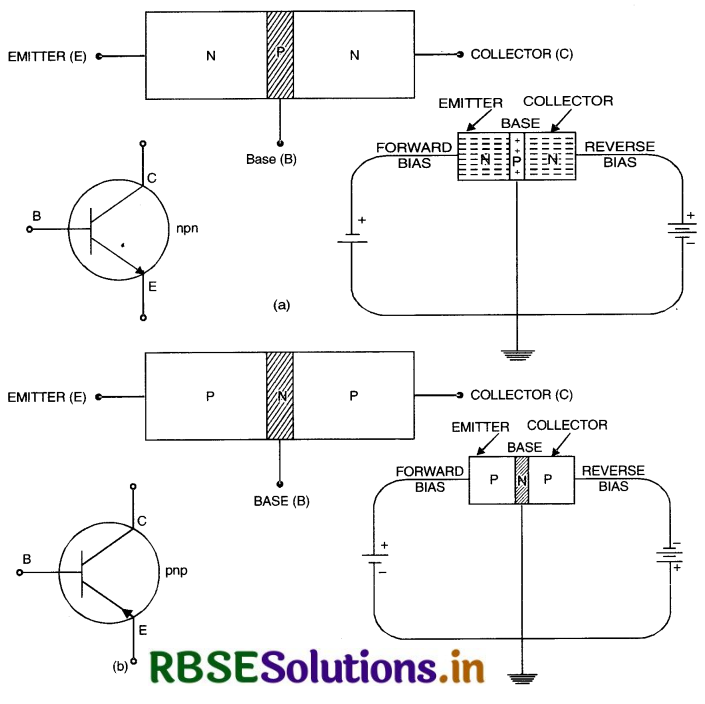
Question 18.
Discuss the action of a (i) n-p-n transistor (ii) p-n-p transistor.
Answer:
(i) Action of n-p-n Transistor. The base-emitter junction is forward biased and the base-collector junction is reverse baised. Since the base- emitter junction is forward biased, a large number of electrons from the emitter are injected into the base region. One expects this large current of electrons to flow out of the p-type base region and to constitute a large base current. But the base region is so thin that an electron is very unlikely to recombine with a hole from the p-type base region (the thickness of the base region typically less than 10-3 cm). However, 2% to 5% electrons are lost in recombination the rest 95 to 98% free electrons cross the collector base junction. These electrons passing through type p-type base region are pulled inside the collector region and form the collector current (LAQ LAQ 18).
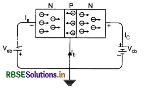
Almost all electrons emitted from the emitter are collected by the collector. Consider the base current. It is due to the small fraction of electrons which recombine in the base region. This base current (IB) will therefore necessarily be a small fraction (typically ≤ 1%) of the collector current (Ic).
Therefore, we see the following:
(1) The emitter current (Ie) is the sum of the base current and the collector current:
Ie ≃ Ib + Ic
(2) The collector current is smaller than the emitter current Ic < Ie or, Ib << Ic. Further, Ib is a fixed small fraction of Ic, this fraction being determined by the shape of the transistor, doping levels, bias voltages etc.
Working of n-p-n
In working of n-p-n transistor, the current is constituted by electrons. As each electron reaches the collector electron, it enters the positive terminal and simultaneously an electron is ejected into the emitter from the forward biased. This process is repeated maintaining continuous supply of electrons.
(ii) Action of p-n-p Transistor. In a p-n-p transisor, when the emitter is forward biased, the holes in the emitter and the electrons in the base begin to move towards the junction, holes being attracted by the negative terminal and the electrons by the positive terminal of the battery. On reaching the base-emitter junction a small fraction of total number of holes with electrons to get neutralized. As the base layer is very thin the collector is kept at high negative potential, almost all the holes are attracted by the collector, producing a hole-current between the emitter and collector (Fig. LAQ 18 (b)).
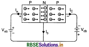
The emitter current Ie is the sum of base current and the collector current.
i.e. Ie = Ib + Ic
So Ic < Ie
Working of p-n-p
In working of p-n-p, as each hole reaches the collector an electron is emitted from the negative terminal of battery and the hole is neutralized. Simultaneously a covalent bond is broken near the emitter electron the electron so produced enter the positive terminal of the forward bias battery and the hole starts its journey towards the emitter base junction. Holes are the current carriers in p-n-p transistor, however the current in the outer circuit is always due to flow of electrons.
Question 19.
Define the following terms in regard to a transistor:
(a) Current gain
(b) Resistance gain
(c) Voltage gain
(d) Power gain
(e) Transistor conductance.
Answer:
(a) Current gain (a). Current amplification factor ‘a’ is defined as a ratio of small change in the collector current to the small change in the emitter current at constant collector voltage.
Thus, a = \(\left(\frac{\delta \mathrm{I}_c}{\delta \mathrm{I}_e}\right)\) with Ec constant
(b) Resistance gain. The resistance gain of a transisor is defined as the ratio of collector-base internal resistance to the emitter-base internal resistance. Thus
Resistance gain = \(\frac{\mathrm{R}_o}{\mathrm{R}_i}\)
(c) Voltage gain. The collector circuit, being reverse biased, has very high internal resistance. This permits a high load resistance R, to be inserted in the collector circuit, without affecting the output current and this is the basis of voltage amplification in a transistor.
For the sake of explanation, let us consider a p-n-p common base junction transistor having a current gain a. Let an input signal voltage be fed to the emitter-base circuit having the low input.
Emitter Current, Ie = \(\frac{\mathrm{V}_i}{\mathrm{R}_i}\)
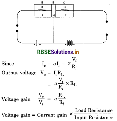
(d) Power gain. It is defined as the ratio of the output power to input power.
Power gain = \(\frac{\text { Output power }}{\text { Input power }}\)
= \(\frac{\mathrm{I}_e \times \mathrm{R}_e}{\mathrm{I}_e \times \mathrm{R}_i}\)
= a2 x Resistance gain
(e) Transistor conductance. Transistor conductance is defined as the ratio of change in collector current to change in base emitter voltage.
gm = \(\frac{\Delta \mathrm{I}_c}{\Delta \mathrm{V}_{b c}}\)
The quantity gm has units of conductance and is called the transfer conductance or transconductance of the transistor. The transconductance of a transistor depends upon the geometry, doping levels and biasing of the transistor.
Question 20.
What are characteristics of a transistor? Give the input and output characteristics of common emitter.
Answer:
Characteristics of transistor.
Graphical representation of the variation among various voltages and currents in a transistor is called transistor characteristics.
Since a transistor has three sections, emitter, base and collector, each transistor circuit must have an input circuit containing two terminals and an output circuit containing two terminals, so one of the section must be common to both the input and output circuits. Hence there are three types of characteristics of a transistor.
- common base characteristics
- common emitter characteristics
- common collector characteristics
These characteristics have their own advantages and disadvantages. The slope of each characeristic may give a transistor parameter. In all the above three characteristics the emitter is always forward baised and collector is always reverse biased. Common base and common collector characteristics are sufficient to understand the behaviour of the device and common collector characteristics of a transistor are usually not needed and common collector characteristics can be taken as special case of common emitter configuration. Transistor characteristics are shown in Fig. LAQ 20.
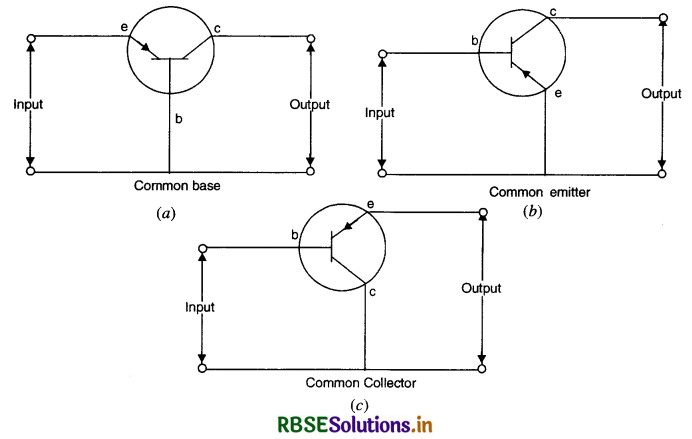
Question 21.
Describe an experimental set up for drawing common base characteristics of p-n-p junction transistor. Discuss their shape. What do you conclude from them?
Answer:
Common base characteristics. The circuit diagram for common base p-n-p transistor is shown in Fig. LAQ 21 (a). The input is applied across the emitter and base and output is taken across collector and base. Here base is common to both the input and output circuits. The most important characteristics of common base connections are input characteristics and output characteristics.
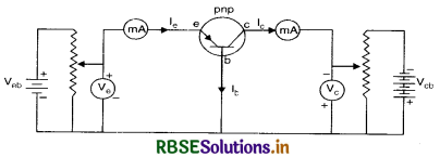
(i) Input characteristics (or emitter characteristics). A graph showing the relationship between the emitter-base voltage and the emitter current at constant collector base voltage is called input characteristics or emitter characteristics of the transistor. To obtain input characteristics, the emitter base circuit is forward biased by emitter to base voltage Veb and collector base circuit is reverse baised by collector to base voltage Vcb. The collecor voltage Vcb is kept constant at a suitable value. The emitter voltage Veb is varied in small steps and the emitter current Ie is noted corresponding to each value of the emitter voltage. A curve is then plotted between Veb and Ie for a given value of V. This is one characteristic. Similar characteristic curves can be drawn for different fixed values of Vcb as shown in Fig. LAQ 21 (b)
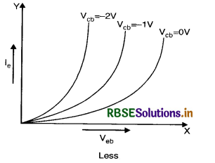
(ii) Output Characteristics (or collector characteristics). A graph showing the relationship between the collector base voltage and collector current at constant emitter current is called the collector characteristic or the output characteristic of the transistor. To obtain output characteristics, the emitter current Ie is kept constant at a suitable value. The collector voltage Vcb is varied in small steps and the collector current Ic is noted corresponding to each value of the emitter current. A curve is then plotted between Vcb and Ic for a given value Ie. This is one characteritics. Similar characteristic curves can be drawn for different fixed values of Ic as shown in Fig. LAQ 21 (c).
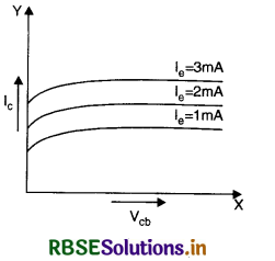
Conclusions
From input characteristic
- We find that the emitter current rises rapidly with small increase in emitter voltage i.e. input resistance of emitter base circuit is low.
- As Vb is made more negative, more holes are attracted by collector, so emitter current Ie rises more rapidly.
From output characteristics
- We find that for a given value of emitter current Ie, the collector current is not zero when Vcd = 0.
- A very large change in the collector base voltage Vcb produces only a small change in the collector current i.e. output resistance is very high.
Question 22.
Describe an experimental set up for drawing common emitter characteristics of p-n-p junction transistor. Discuss their shapes. What do you conclude from them?
Answer:
Common emitter characteristics. The circuit diagram for common emitter p-n-p transister is shown in Fig. (a). The input is applied across the emitter and base and output is taken across collector and emitter. Here emitter is common to both input and output circuits. The most important characteristics of common emitter connections are input characteristics and output characteristics.
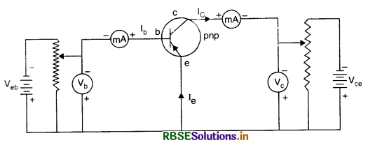
(i) Input characteristics
As graph showing the relationship between base-emitter voltage and base current and constant collector-emitter is called input characteristics of the transistor. To obtain input characteristic, the emitter is forward biased by base emitter voltage Vbe and the collector is reverse baised by collector emitter voltage Vce. The collector voltage Vce is kept constant at a suitable value. The base voltage Vbe is varied in small steps and the base current Ib is noted corresponding to each value of the base-emitter voltage. A curve is then plotted between Vbe and Ib for a given value of Vce. This is one characteristic. Similar characteristic curves can be drawn for diferent fixed values of Vce (say OV, - 2 V, - 4V etc.) as shown in Fig. LAQ 22 (b).
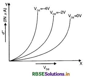
(ii) Output characteristics
A graph showing the relationship between the collector emitter voltage and collector current at different constant base current is called output characteristic of the transistor. To obtain output characteristics the base current is kept constant at a suitable value the collector-emitter voltage Vce is varied in small steps and collector current Ic is noted corresponding to each value of base current Ib. A curve is then plotted between Vce and Ic for a given constant value of Ib. This is one characteristics. Similar characteristic curves can be drawn for diferent values of Ib (say 10 mA, 15mA, 20mA, etc. as shown in fig. LAQ 22 (c))
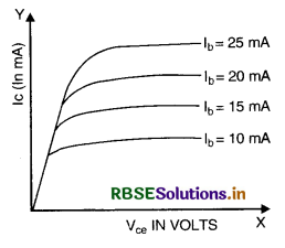
Conclusions
From input characteristics
- Base current increases non-linearly with increase in base voltage.
- Base current increases less rapidly with base-emitter voltage as compared to common base characteristics.
- The input characteristics slightly depend on the collector-emitter voltage.
From output characteristics
- For a given value of collector voltage, Ic is large for larger value of Ib.
- At low value of base current, the collector voltage has little effect on the collector current but at higher value of base current, the collector current is almost independent of collector voltage.
Question 23.
Explain with the help of labelled circuit diagram, the use of n-p-n Transisor as an amplifier in common base configuration. Why is common base amplifier preferred over common emitter amplifier.
Answer:
Common base amplifier. The circuit diagram for common base n-p-n transistor is as shown in Fig. LAQ 23 (n-p-n transistor is being used to explain the basic principle because of its simplicity). In this circuit the base lead is common to both the input (emitter-base) and output (Collector-base) circuit and is grounded. The emitter is forward biased by emitter base battery Veb and collector is reversed biased by collector base battery Vec, so output resistance is more input resistance i.e. R0 > Ri. The input signal is applied across emitter-base and output voltage is obtained across a load RL between collector and base in series with collector battery.
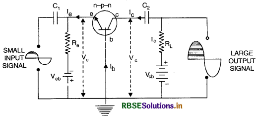
Let Ie, Ib and Ic be emitter, base and collector current respectively,
so Ie = Ib + Ic ........................(1)
The potential drop across load RL is IcRL
so Vc = Vcb - IcRL ......................(2)
When ac signal is fed to the input circuit, let the first half cycle of input voltage is +ve. It will make emitter less negative and hence emitter current decreases. Hence IcRL factor decreases. From eq. (2) we find that collector voltage Vc will increase. So corresponding to positive half cycle of a.c. input, positive output Half cycle will be obtained.
During second half cycle of a.c. input voltage will be negative and it will make emitter more negative, hence emitter current decreases. So IcRL factor also increases. From Fig. LAQ 23 we find that collector voltage Vc will decrease. So corresponding to negative half cycle of ac input negative output half cycle will be obained.
Thus, in common base amplifier, the output voltage is in phase with the input signal. Since input circuit has low resistance (30 to 50 Ω) and output circuit has high resistance (≅ 500 kΩ), so a large a.c. voltage will be developed across the load corresponding to a small change in the input voltage, so the signal gets amplified.
1. a.c. current gain (αa.c)
the ratio of the change in the collector current to the change in emitter current at constant collector voltage is called ac current gain. Hence,
αa.c. = \(\left(\frac{\Delta I_c}{\Delta I_e}\right)_{V_c}\) .........................(3)
2. d.c. current gain (αd.c)
The ratio of collector current to the emitter current at constant collector, collector voltage is called dc current gain. Hence,
αd.c. = \(\left(\frac{I_c}{I_e}\right)_{V_c}\) ............................(4)
αd.c. is very nearly equal to αa.c., so we generally denote the current gain as α. Unless otherwise specified α means ac current gain. α is slightly less than 1 because collector current is slightly less than emitter current.
3. Voltage gain (Av)
The ratio of change of output voltage to the change in input voltage is called voltage gain. Hence,
Av = \(\frac{\Delta \mathrm{V}_0}{\Delta \mathrm{V}_i}=\frac{\mathrm{I}_c \mathrm{R}_{\mathrm{L}}}{\mathrm{I}_e \mathrm{R}_i}=\alpha \frac{\mathrm{R}_{\mathrm{L}}}{\mathrm{R}_i}\)
So, Av = α (Resistance gain) .........................(5)
Since RL >> Ri, So Av is quite high although α < 1.
4. Power gain (p)
The ratio of change of output power to the change in input power is called power gain. Hence,
Power gain = Voltage x Current gain
P = α.\(\left(\frac{\mathrm{R}_{\mathrm{L}}}{\mathrm{R}_i}\right)\).α
So, Power gain P = a2 (Resistance gain) .....................(6)
Power gain is moderate.
Question 24.
With the help of a labelled diagram, explain how an n-p-n transistor can be used as an amplifier in common emitter configuration. Explain how the input and output voltages are out of phase by 180° for a common emitter transistor amplifier.
Answer:
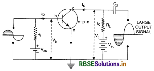
Common emitter Transistor amplifier
The circuit diagram for common emitter n-p-n amplifier is as shown in Fig. LAQ 24. In this circuit, the emitter lead is common to both the input (emitter-base) and output (collector-emitter) circuit and is grounded. The emitter is forward biased by emitter base battery Veb and collector is reversed biased by collector-emitter battery Vec, so output resistance is more than input resistance i.e. R0 >> Ri.
Let Ie, Ib and Ic be emitter, base and collector current respectively.
So Ie = Ib + Ic ............................(1)
If RL is load resistance, then the potential drop across RL is IcRL
Hence, collector voltage
Vc = Vec - IcRL .........................(2)
When a.c. is fed to the input signal let the first half cycle of input voltage is positive. It will make base more positive and hence emitter current will increase and correspondingly collector current also increases. Hence IcRL factor increases from eq. (2) we find that collector voltage will decrease. Thus corresponding to positive half cycle of a.c. input signal, negative output half cycle will be obtained.
During second half cycle of a.c. input, voltage will be negative and it will make base more negative which decreases the emitter current and hence collector current lc also decreases. So IcRL factor also decreases. From eq. (2) we find that collector voltage will decrease. Thus corresponding to negative half cycle of a.c. input signal, positive output half cycle will be obtained.
Thus in common emitter amplifier the output voltage signal are out of phase with each other as shown in Fig. LAQ 24 since input resistance is moderately low (1-2 kΩ) and the output resistance is moderately high (≅ 50 kΩ), so the collector current (output current is very large as compared to base current (input current).
1. Ac current gain (ßa.c.)
The ratio of change in collector current to the change in base current at constant collector voltage. Hence,
ßac = \(\left(\frac{\Delta I_c}{\Delta I_b}\right)_{V_c}\) ..............................(3)
2. d.c. current gain (ßd.c)
The ratio of collector current to the base current at constant collector voltage is called dc current gain. Hence,
ßd.c. = \(\left(\frac{\mathrm{I}_c}{\mathrm{I}_b}\right)_{\mathrm{V}_c}\) ...............................(4)
ßd.c. is very nearly equal to ßa.c., so we generally denote the current gain in CE mode as ß. Unless otherwise specified ß means ac current gain. The value of ß varies from 20 to 50.
3. Voltage gain (Av)
The ratio of change in output voltage to the change in input voltage is called voltage gain.
i.e. Av = \(\frac{\Delta \mathrm{V}_0}{\Delta \mathrm{V}_b}=\frac{\Delta \mathrm{I}_c}{\Delta \mathrm{I}_b} \cdot \frac{\mathrm{R}_{\mathrm{L}}}{\mathrm{R}_i}\)
or Av = ß.\(\frac{\mathrm{R}_{\mathrm{L}}}{\mathrm{R}_i}\) .............................(5)
or Av = ß (resistance gain)
Which is higher than that obtained in case of common-base transisor amplifier.
4. Power gain (P)
The ratio of change in output power to the change in input power is called power gain. Hence,
Power gain = voltage gain x current gain
= ß\(\left(\frac{\mathrm{R}_{\mathrm{L}}}{\mathrm{R}_i}\right)\) x ß
So, power gain P = ß2 (Resistance gain)
= very high power gain ................................(6)
Question 25.
Derive a relation between α and ß of a transistor.
Answer:
For n-p-n and for p-n-p transistor we have
Ie = Ib + Ic
∴ ∆Ie = ∆Ib + ∆Ic
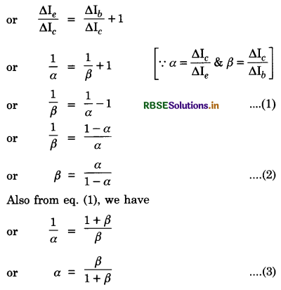
Question 26.
(a) What do you mean by LC oscillations?
(b) Draw circuit diagram showing use of a transistor as an oscillator.
Answer:
(a) LC oscillations. An LC circuit can be used to produce oscillations of desired frequency. It consists of a tank circuit containing an inductor L and capacitor C connected in parallel.
The frequency of the tank circuit is given by
v = \(\frac{1}{2 \pi \sqrt{L C}}\)
Due to the resistance of inductive coil, there occurs a small but constant energy loss and oscillations thus produced are damped. To transmit speech or music, we require undamped electromagnetic waves called carrier waves. To do so an LC circuit is coupled with transistor in such a way that there is a proper feedback to the LC circuit at the time so that the energy of LC circuit remains the same throughout oscillations.
(b) Transistor as an oscillator. An oscillator is an electronic device which converts direct current into alternating current of high frequency and constant amplitude.
Circuit diagram
Fig. LAQ 26 shows the circuit diagram for a n-p-n transistor as an oscillator in common-emitter configuration. Common-emitter circuit is reverse biased by battery E. A coil L' is inserted in collector-emitter circuit and it is coupled with L which is connected in the emitter-base circuit.
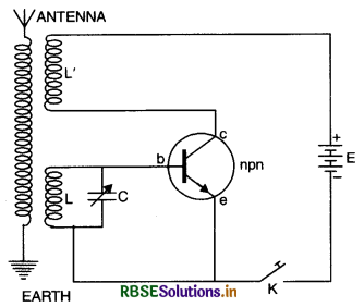
Working. When key K is closed, a small collector current start rising through L' and a change in electric current hence change in magnetic flux in L' is produced so a small induced e.m.f. is produced in L which is coupled with L'. Thus a small current flows in the emitter-base circuit. If it produces forward biasinig in this circuit, then small emitter current causes a corresponding increase in the collector current and upper plate of capacitor C gets positively charged and more magnetic flux is linked with L' and hence with L, so emitter current is further increased. This process continues till collector current becomes saturated.
As the current reaches saturation value, the mutual inductance stops playing its part. The capacitor C gets discharged through inductance L, and emitter current falls, so collector current also falls and a decreasing magnetic flux is linked with coil L' and hence with L. The decreasing collector current induces voltage in L its reverse direction which decreases the emitter current further. Now the lower plate of the capacitor is positively charged. This process continues till collector current becomes zero. Again mutual inductance stops playing its part. The capacitor gets discharged through inductance L and emitter current increases. The whole process will be repeated again and again.
The frequency of oscillations produced will be given by
v = \(\frac{1}{2 \pi \sqrt{L C}}\)
The frequency v can be varied by changing the value of capacitor C by a variable capacitor.
Question 27.
Define a sinusoidal analogue signal and digital signal.
Answer:
Analogue signal. A continuous time varying voltage or current signal is called analogue signal. Analogue devices are ammeter which is used to measure current and a voltmeter which is used to measure voltage etc. Fig. LAQ 27 (a) shows a voltage signal varying sinusoidally.
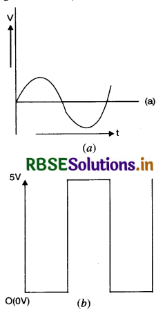
Digital signals. In digital circuits two level of voltages (represented by 0 or 1) are called digital signal.
The word digital means that the information is represented by variables that take a limited number of discrete values. In digital signals, the pulse waveform has only two values 0 and 1 and does not vary continuously with time as in analogue voltage signal. Fig. LAQ 27 (b) shows a digital voltage signals. Here corresponding to binary number 0, the voltage 0 V and corresponding to binary number 1, the voltage is 5 V. The computers, counters etc, all use digital signals.
Question 28.
With the help of labelled circuit diagram, explain the working of transistor as a switch.
Answer:
Transistor as a switch Circuit diagram. The circuit diagram of an n-p-n transistor in CE mode is as shown in the figure LAQ 28 (a). In this circuit, the emitter is forward biased by emitter-base battery Vbb and the collector is reversed biased by emitter collector battery Vcc. RB and Rc are input and output resistances connected between emitter-base and collector-base respectively. Using Kirchhoffs law,
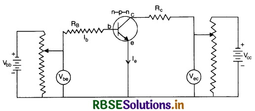
In emitter-base circuit
Vbb = Vbe + IbRB .............................(i)
In collector-base circuit,
Vec = Vce - IcRc ...............................(ii)
Here Vbb = Vi (input voltage) and
Vec = V0 (output voltage)
∴ Vi = Vbe + IbRB ..............................(iii)
V0 = Vcc - IcRc .........................(iv)
Equations (iii) and (iv) indicate how V0 changes when Vi is increased slowly, (for Si n-p-n transistor)
(i) If Vi < 0.6 V, the transistor is in cut off state and Ic = 0 and V0 = Vcc.
(ii) If 0.6 V < Vi < 1 V the transistor is in active state and Ic increases linearly and V0 is less than the earlier value of Vcc.
(iii) If Vi > 1 V, Ic increases non-linearly and hence V0 decreases non-linearly and when IcRc becomes maximum and transistor is said to be in saturation state tending to zero as shown in figure LAQ 28(b).
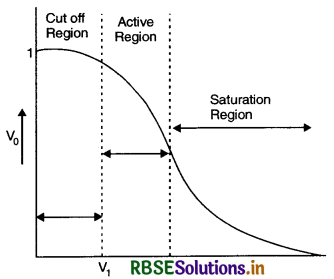
Switching action
(i) When input voltage is very small, the transistor is in cut off region i.e. the transistor is not conducting and acts as if in open condition i.e. OFF state.
(ii) When input voltage is large and the transistor is in saturation state, V0 is very small (V0 ≃ 0), the transistor acts as a closed switch i.e. ON state.
Question 29.
(a) With the help of the circuit diagram explain the working principle of a transistor amplifer as an oscillator.
(b) Distinguish between a conductor, a semiconductor and an insulator on the basis of energy band diagrams.
Answer:
(a) Transistor as an oscillator. An oscillator is an electronic device which converts direct current into alternating current of high frequency and constant amplitude.
Circuit diagram
Fig. LAQ 26 shows the circuit diagram for a n-p-n transistor as an oscillator in common-emitter configuration. Common-emitter circuit is reverse biased by battery E. A coil L' is inserted in collector-emitter circuit and it is coupled with L which is connected in the emitter-base circuit.

Working. When key K is closed, a small collector current start rising through L' and a change in electric current hence change in magnetic flux in L' is produced so a small induced e.m.f. is produced in L which is coupled with L'. Thus a small current flows in the emitter-base circuit. If it produces forward biasinig in this circuit, then small emitter current causes a corresponding increase in the collector current and upper plate of capacitor C gets positively charged and more magnetic flux is linked with L' and hence with L, so emitter current is further increased. This process continues till collector current becomes saturated.
As the current reaches saturation value, the mutual inductance stops playing its part. The capacitor C gets discharged through inductance L, and emitter current falls, so collector current also falls and a decreasing magnetic flux is linked with coil L' and hence with L. The decreasing collector current induces voltage in L its reverse direction which decreases the emitter current further. Now the lower plate of the capacitor is positively charged. This process continues till collector current becomes zero. Again mutual inductance stops playing its part. The capacitor gets discharged through inductance L and emitter current increases. The whole process will be repeated again and again.
The frequency of oscillations produced will be given by
v = \(\frac{1}{2 \pi \sqrt{L C}}\)
The frequency v can be varied by changing the value of capacitor C by a variable capacitor.
(b) In insulator. In insulators, valence band is completely filled and conduction band is completely empty. The energy gap (Eg) between the two is so large that the electrons cannot overcome it and, hence, conduction is not possible. Therefore, insulators are poor conductors of electricity. Electrons cannot gain energy from the applied field and current cannot flow. An important example of insulator is diamond with energy gap of about 5.4 eV (Fig. LAQ 2 (a))

Semiconductors
The energy and structure of a semi conductor is shown in Fig. LAQ 2 (b) It is similar to that of an insulator but with a comparatively small energy gap of about 1 eV. At absolute zero of temperature, the conduction band of semiconductor is totally empty, and all the energy states in the valence band are filled. The absence of electrons in the conduction band at absolute zero does not allow current to flow under the influence of an electric field. Therefore, they are insulators at low temperatures.
However, at room temperature, some valence electrons acquire thermal energy greater than the energy gap Eg and move to the conduction band where they are free to move under the influence of even a small electric field. Common examples of semiconductors are silicon (14), Germanium (32) with energy gap of about (1.12 eV) and 0.75 eV respectively. The gap (band) that separates conduction and valence band is called Forbidden Band.
Metals (Conductors)
The energy band structure of a metal is shown schematically in Fig. LAQ 2 (c). The last occupied band of energy levels is only partially filled:
The available electrons occupy, one by one (Pauli exclusion principle) the lowest levels. This leaves part of the band (called conduction band unoccupied.
The highest energy level occupied at absolute zero by electrons is partially filled conduction band, is called Fermi level and the corresponding energy is called Fermi energy.
When an electric field is applied, electrons gain energy (about 108 eV). They can be excited to empty energy levels immediately about the Fermi level and some of the electrons are accelerated in the direction of the field. Thus electric current is conducted through the conductors.
Question 30.
(i) Draw a circuit diagram to study the input and output characteristics of a n-p-n transistor in its common emitter configuration. Draw the typical input and output characteristics.
(ii) Explain, with the help of a circuit diagram, the working of n-p-n transistor as a common emitter amplifier.
Answer:
(i) Common emitter characteristics. The circuit diagram for common emitter n-p-n transistor is shown in Fig. LAQ 30 (a). The input is applied across the emitter and base and output is taken across collector and emitter. Here emitter is common to both input and output circuits. The most important characteristics of common base connections are input characteristics and output characteristics.
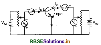
(a) Input characteristics
A graph showing the relationship between base-emitter voltage and base-current and different constant collector-emitter is called input characteristics of the transistor.
To obtain input characteristic, the emitter is forward biased by base emitter voltage Vbe and the collector is reverse biased by collector emitter voltage Vce. The collector voltage Vce is kept constant at a suitable value. The base voltage Vp is varied in small steps and the base current Ib is noted corresponding to each value of the base-emitter voltage. A curve is then plotted between Vbe and Ib for a given value of Vce. This is one characteristic. Similar characteristic curves can be drawn for different fixed values of Vce (say 2V, 3V, 4V etc.,) as shown in Fig. LAQ 30 (b)

(b) Output Characteristics
A graph showing the relationship between the collector emitter voltage and collector current at constant base curent is called output characteristics of the transistor.

To obtain output characteristics the base current is kept constant at a suitable value the collector-emitter voltage Vce is varied in small steps and the collector current Ic is noted corresponding to each value of the base current Ib. A curve is then plotted between Vce and Ic for a given constant value of Ib. This is one characteristic. Similar characteristic curves can be drawn for different fixed values of Ib (say 10µA, 15 µA, 20 µA etc. as shown in Fig. LAQ 30 (c).
(ii)

Common emitter Transistor amplifier
The circuit diagram for common emitter n-p-n amplifier is as shown in Fig. LAQ 24. In this circuit, the emitter lead is common to both the input (emitter-base) and output (collector-emitter) circuit and is grounded. The emitter is forward biased by emitter base battery Veb and collector is reversed biased by collector-emitter battery Vec, so output resistance is more than input resistance i.e. R0 >> Ri.
Let Ie, Ib and Ic be emitter, base and collector current respectively.
So Ie = Ib + Ic ............................(1)
If RL is load resistance, then the potential drop across RL is IcRL
Hence, collector voltage
Vc = Vec - IcRL .........................(2)
When a.c. is fed to the input signal let the first half cycle of input voltage is positive. It will make base more positive and hence emitter current will increase and correspondingly collector current also increases. Hence IcRL factor increases from eq. (2) we find that collector voltage will decrease. Thus corresponding to positive half cycle of a.c. input signal, negative output half cycle will be obtained.
During second half cycle of a.c. input, voltage will be negative and it will make base more negative which decreases the emitter current and hence collector current lc also decreases. So IcRL factor also decreases. From eq. (2) we find that collector voltage will decrease. Thus corresponding to negative half cycle of a.c. input signal, positive output half cycle will be obtained.
Thus in common emitter amplifier the output voltage signal are out of phase with each other as shown in Fig. LAQ 24 since input resistance is moderately low (1-2 kΩ) and the output resistance is moderately high (≅ 50 kΩ), so the collector current (output current is very large as compared to base current (input current).
1. Ac current gain (ßa.c.)
The ratio of change in collector current to the change in base current at constant collector voltage. Hence,
ßac = \(\left(\frac{\Delta I_c}{\Delta I_b}\right)_{V_c}\) ..............................(3)
2. d.c. current gain (ßd.c)
The ratio of collector current to the base current at constant collector voltage is called dc current gain. Hence,
ßd.c. = \(\left(\frac{\mathrm{I}_c}{\mathrm{I}_b}\right)_{\mathrm{V}_c}\) ...............................(4)
ßd.c. is very nearly equal to ßa.c., so we generally denote the current gain in CE mode as ß. Unless otherwise specified ß means ac current gain. The value of ß varies from 20 to 50.
3. Voltage gain (Av)
The ratio of change in output voltage to the change in input voltage is called voltage gain.
i.e. Av = \(\frac{\Delta \mathrm{V}_0}{\Delta \mathrm{V}_b}=\frac{\Delta \mathrm{I}_c}{\Delta \mathrm{I}_b} \cdot \frac{\mathrm{R}_{\mathrm{L}}}{\mathrm{R}_i}\)
or Av = ß.\(\frac{\mathrm{R}_{\mathrm{L}}}{\mathrm{R}_i}\) .............................(5)
or Av = ß (resistance gain)
Which is higher than that obtained in case of common-base transisor amplifier.
4. Power gain (P)
The ratio of change in output power to the change in input power is called power gain. Hence,
Power gain = voltage gain x current gain
= ß\(\left(\frac{\mathrm{R}_{\mathrm{L}}}{\mathrm{R}_i}\right)\) x ß
So, power gain P = ß2 (Resistance gain)
= very high power gain ................................(6)
Question 31.
How is a zener diode fabricated so as to make it a special purpose diode? Draw I-V characteristics of zener diode and explain the significance of breakdown voltage.
Explain briefly, with the help of a circuit diagram, how a p-n junction diode works as a half wave rectifier.
Answer:
Zener diode.
The Zener diode
A specially designed p-n junction diode which has a sharp breakdown voltage is called a zener diode. The current that flows under reverse breakdown is not necessarily destructive if the amount is limited to a value such that the diode does not become overheated. By suitably controlling the amount of impurity and making the p-n junction free from surface imperfections, the voltage at which breakdown takes place can be made to occur very distinctly and sharply, as shown in Fig. LAQ 15. This type of diode is called a

zener diode and the breakdown voltage Vz is called Zener Voltage.
Zener voltage depends upon the amount of doping. If the diode is lightly doped the breakdown voltage has higher value and if it is heavily doped, the breakdown voltage will occur at a lower value.
The following points may be noted about he zener diode.
(i) A zener diode is always reverse biased.
(ii) A zener diode has sharp breakdown voltage called zener voltage Vz.
(iii) A zener diode is like a conventional diode except that it is properly doped to have a sharp breakdown voltage.
(iv) In forward bias-conditions, a zener diode acts like a conventional p-n junction diode.
(v) The zener diode is not immediately burnt simply because it has entered the breakdown region. As long as the external circuit connected to the diode limits the diode current to less than burnt out value, the diode will not burn out.
(vi) Temperature Coefficient
The temperature coefficient is defined as the percentage change in reference voltage per degree Celsius change in diode temperature. These data are supplied by the manufacturer. The coefficient may be either positive or negative and will normally be in the range ±0.1 per cent/°C. If the reference voltage is above 6 V, where the physical mechanism involved is avalanche multiplication, the temperature coefficient is positive. However, below 6V, where true zener-breakdown is involved, the temperature coefficient is negative.
Uses.
Zener diodes find numerous applications in transister circuitry. Most important of them are:
- as voltage regulators.
- as a fixed reference voltage in a network for biasing and comparison.
- for calibrating voltmeters.
- for avoiding meter damage by accidental application of excessive voltage.
Circuit arrangement
The basic circuit for half wave rectifier is as shown in Fig. LAQ 11 (a). Most electronic equipments have a transformer at the input. The transformer allows us to step the voltage up or down to get desired level of d.c. voltage and can provide isolation from the power line and thus reduces the risk of electrical shock. The a.c. supply to be rectified is applied to the primary (P) of a transformer. The secondary (S) is connected in series with the diode and the load resistance RL. The d.c. output is obtained across the load Rl. Since diode conducts only for half cycle of the a.c. voltage applied (i.e. when forward biased), and does not conduct for the negative half cycle, thus in this case it is known as half wave rectifier.

Theory
During positive half of input a.c., the point A is positive and B is negative. The diode D2 and D3 are forward biased and conduct, while D1 and D4 are reverse biased and do not conduct. These two diodes are in series through the load RL and the direction of conventional current is shown by full arrows.
(ii) Peak inverse voltage is shared by one diode. So this rectifier cannot be used for high voltages.
(ii) Bridge Rectifier
Bridge rectifier is the most widely used of all the rectifiers. It is a full wave rectifier and does not require centre tapped transformer.
Circuit arrangement
It consists of four diodes D1, D2, D3, and D4 which are connected to form a bridge as shown in Fig. LAQ 11 (e). The a.c. supply to be rectified is applied to the diagonally opposite ends of the bridge through the transformer and the load resistance RL is connected between the other two ends of the bridge.
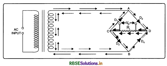

During negative half of input a.c., the point B is positive and A is negative. The diodes D1 and D4 are forward biased and conduct while D2 and D3 are reverse biased and do not conduct. These two diodes are in series through the load RL and the direction of conventional current is shown by dotted arrows. We find that whether diodes D2 and D3 conduct or D4 and D4 conduct, the direction of current in both the half cycles along the load RL is always from D to C. The waveform of input and output voltage is as shown in Fig. LAQ 11 (f).
Advantages
- Centre tapped transformer is not required.
- The full voltage of secondary is applied across the two conducting diodes. So the output is twice that of the centre tap circuit for the same secondary voltage.
- Peak inverse voltage is half that of conventional centre tap rectifier.
Disadvantages
- It is un-economical as it requires four diodes.
- Since during each half cycle of a.c. input two diodes that conduct are in series. So voltage drop across the internal resistance of the diodes is double of the value in the centre tap circuit and thus the efficiency of the bridge rectifier is very low.
Question 32.
What are energy bands? How they are formed? Distinguish between a conductor, an insulator and a semiconductor on the basis of energy band diagram.
Answer:
In an atom, the electrons revolve around the nucleus in almost circular orbits (Bohr’s model). Energy of electrons in each subshell is definite. These definite energy values are called energy levels of the atoms. But in crystals, atoms are arranged in a regular and periodic manner. A solid crystal contains about 1023 atoms/cm3. So each atom is in the electrostatic field of neighbouring atoms and due to interaction between the atom, the modification of energy level takes place. The maximum effect of the interaction is on the valence electron and the energy E between E + ∆E. Thus each energy level becomes broad. This broadening of energy level is called energy band. The electrons in the inner shell are strongly bound to the nuclei, so they are slightly affected by the presence of neighbouring atoms. They are called core levels. If an energy bond consists of as much electrons as permitted by Pauli’s Exclusion Principle, then it is said to be completely filled band, and in such a band there will be no free electrons for conduction of electricity, while for a partially filled band conduction is possible.
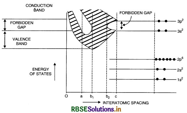
In order to understand how the modification of energy level takes place, let us consider a single crystal of Si having N atoms. The electronic configuration of Si is 1s2, 2s2, 2p6, 3s2, 3p2. The energy levels of Si atom in isolated state as well as in the crystal form are shown in Fig. 14.85. Here the interatomic spacing is r and distance ‘a’ corresponds to the crystal lattice spacing. The process of splitting is summarised as follows:
1. When r > c.
The atomic spacing is sufficiently wide, so the interaction between atoms is negligible and practically, here is no modification of 3s and 3p energy sublevels.
2. When r = c.
When atoms are brought further close to each other, their interaction increases and the real splitting of the sublevels starts. The energy difference between 3s and 3p sublevels is denoted by double arrow and is called forbidden gap.
3. When r < c.
The forbidden gap decreases and reduces to zero at r = b2. So at r = b2 the two bands overlap. At a distance between b2 and c instead of single 3s or 3p level, we get a large number of closely packed levels. The number N is very large so this collection of closely spaced levels is called an energy band.
4. When b1 < r < b2.
When the atomic spacing is further reduced, the 3s and 3p levels remain merged into each other and thus there is no restriction on the electrons to move from 3s sublevels to 3p sublevel or vice versa. The energy gap between 3s and 3p disappears, and the two band overlap. In this situation all 8N levels (2 from s and 6 from p) are now continuously distributed. Here we cannot distinguish between the electrons belonging to 3s and 3p sublevels. At such a situation one can only say that 4N sublevels are filled and 4N sublevels are empty.
5. When r = a.
This is known as equilibrium distance because the atoms in crystal lie at this interatomic separation. Here is the band divide and spread widely Here we find that band of filled energy level and empty energy level are separated by an energy gap called forbidden gap or forbidden band. The lower band which is completely filled up is known as valence band and the upper band which is normally (at 0 K) empty, is referred to as the conduction band.
The gap between valence band and conduction band is called fobidden band and it is a measure of energy E . Thus E is the amount of energy that should be given to the electron in valence band, so that it could jump to the conduction band. For insulator it is of the order of 5 to 10 eV, and for semiconductor like Ge is about 0.72 eV and for Si it is about 1 eV.
In insulator. In insulators, valence band is completely filled and conduction band is completely empty. The energy gap (Eg) between the two is so large that the electrons cannot overcome it and, hence, conduction is not possible. Therefore, insulators are poor conductors of electricity. Electrons cannot gain energy from the applied field and current cannot flow. An important example of insulator is diamond with energy gap of about 5.4 eV (Fig. LAQ 2 (a))
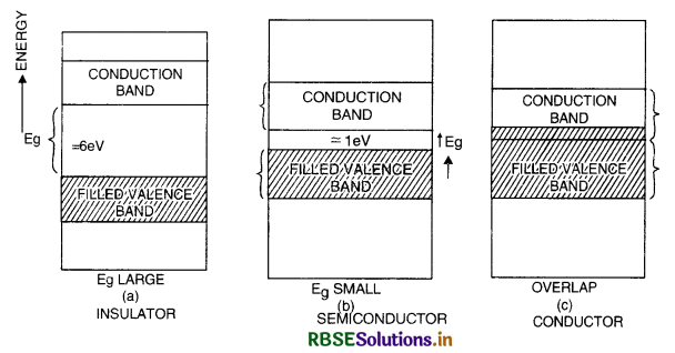
Semiconductors
The energy and structure of a semi conductor is shown in Fig. LAQ 2 (b) It is similar to that of an insulator but with a comparatively small energy gap of about 1 eV. At absolute zero of temperature, the conduction band of semiconductor is totally empty, and all the energy states in the valence band are filled. The absence of electrons in the conduction band at absolute zero does not allow current to flow under the influence of an electric field. Therefore, they are insulators at low temperatures.
However, at room temperature, some valence electrons acquire thermal energy greater than the energy gap Eg and move to the conduction band where they are free to move under the influence of even a small electric field. Common examples of semiconductors are silicon (14), Germanium (32) with energy gap of about (1.12 eV) and 0.75 eV respectively. The gap (band) that separates conduction and valence band is called Forbidden Band.
Metals (Conductors)
The energy band structure of a metal is shown schematically in Fig. LAQ 2 (c). The last occupied band of energy levels is only partially filled:
The available electrons occupy, one by one (Pauli exclusion principle) the lowest levels. This leaves part of the band (called conduction band unoccupied.
The highest energy level occupied at absolute zero by electrons is partially filled conduction band, is called Fermi level and the corresponding energy is called Fermi energy.
When an electric field is applied, electrons gain energy (about 108 eV). They can be excited to empty energy levels immediately about the Fermi level and some of the electrons are accelerated in the direction of the field. Thus electric current is conducted through the conductors.
Question 33.
State the principle of working of p-n-diode as a rectifier. Explain with the help of a circuit diagram, the use of p-n diode as a full wave rectifier. Draw a sketch of the input and output waveforms.
Answer:
(i) p-n junction as half wave rectifier principle
It is based on the principle that in a p-n junction diode the current flows only if it is forward biased and negligible current flows if it is reverse biased.
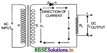
(b) (1) Circuit arrangement
The basic circuit for half wave rectifier is as shown in Fig. LAQ 11 (a). Most electronic equipments have a transformer at the input. The transformer allows us to step the voltage up or down to get desired level of d.c. voltage and can provide isolation from the power line and thus reduces the risk of electrical shock. The a.c. supply to be rectified is applied to the primary (P) of a transformer. The secondary (S) is connected in series with the diode and the load resistance RL. The d.c. output is obtained across the load Rl. Since diode conducts only for half cycle of the a.c. voltage applied (i.e. when forward biased), and does not conduct for the negative half cycle, thus in this case it is known as half wave rectifier.

Theory
During positive half of input a.c., the point A is positive and B is negative. The diode D2 and D3 are forward biased and conduct, while D1 and D4 are reverse biased and do not conduct. These two diodes are in series through the load RL and the direction of conventional current is shown by full arrows.
(ii) Peak inverse voltage is shared by one diode. So this rectifier cannot be used for high voltages.
(ii) Bridge Rectifier
Bridge rectifier is the most widely used of all the rectifiers. It is a full wave rectifier and does not require centre tapped transformer.
Circuit arrangement
It consists of four diodes D1, D2, D3, and D4 which are connected to form a bridge as shown in Fig. LAQ 11 (e). The a.c. supply to be rectified is applied to the diagonally opposite ends of the bridge through the transformer and the load resistance RL is connected between the other two ends of the bridge.


During negative half of input a.c., the point B is positive and A is negative. The diodes D1 and D4 are forward biased and conduct while D2 and D3 are reverse biased and do not conduct. These two diodes are in series through the load RL and the direction of conventional current is shown by dotted arrows. We find that whether diodes D2 and D3 conduct or D4 and D4 conduct, the direction of current in both the half cycles along the load RL is always from D to C. The waveform of input and output voltage is as shown in Fig. LAQ 11 (f).
Advantages
- Centre tapped transformer is not required.
- The full voltage of secondary is applied across the two conducting diodes. So the output is twice that of the centre tap circuit for the same secondary voltage.
- Peak inverse voltage is half that of conventional centre tap rectifier.
Disadvantages
- It is un-economical as it requires four diodes.
- Since during each half cycle of a.c. input two diodes that conduct are in series. So voltage drop across the internal resistance of the diodes is double of the value in the centre tap circuit and thus the efficiency of the bridge rectifier is very low.
Question 34.
(a) With the help of the circuit diagram, explain the working principle of a transistor amplifier as an oscillator.
(b) Distinguish between a conductor, a semiconductor and an insulator on the basis of energy band diagrams.
Answer:
(a) Transistor as an oscillator. An oscillator is an electronic device which converts direct current into alternating current of high frequency and constant amplitude.
Circuit diagram
Fig. LAQ 26 shows the circuit diagram for a n-p-n transistor as an oscillator in common-emitter configuration. Common-emitter circuit is reverse biased by battery E. A coil L' is inserted in collector-emitter circuit and it is coupled with L which is connected in the emitter-base circuit.

Working. When key K is closed, a small collector current start rising through L' and a change in electric current hence change in magnetic flux in L' is produced so a small induced e.m.f. is produced in L which is coupled with L'. Thus a small current flows in the emitter-base circuit. If it produces forward biasinig in this circuit, then small emitter current causes a corresponding increase in the collector current and upper plate of capacitor C gets positively charged and more magnetic flux is linked with L' and hence with L, so emitter current is further increased. This process continues till collector current becomes saturated.
As the current reaches saturation value, the mutual inductance stops playing its part. The capacitor C gets discharged through inductance L, and emitter current falls, so collector current also falls and a decreasing magnetic flux is linked with coil L' and hence with L. The decreasing collector current induces voltage in L its reverse direction which decreases the emitter current further. Now the lower plate of the capacitor is positively charged. This process continues till collector current becomes zero. Again mutual inductance stops playing its part. The capacitor gets discharged through inductance L and emitter current increases. The whole process will be repeated again and again.
The frequency of oscillations produced will be given by
v = \(\frac{1}{2 \pi \sqrt{L C}}\)
The frequency v can be varied by changing the value of capacitor C by a variable capacitor.
(b) In insulator. In insulators, valence band is completely filled and conduction band is completely empty. The energy gap (Eg) between the two is so large that the electrons cannot overcome it and, hence, conduction is not possible. Therefore, insulators are poor conductors of electricity. Electrons cannot gain energy from the applied field and current cannot flow. An important example of insulator is diamond with energy gap of about 5.4 eV (Fig. LAQ 2 (a))

Semiconductors
The energy and structure of a semi conductor is shown in Fig. LAQ 2 (b) It is similar to that of an insulator but with a comparatively small energy gap of about 1 eV. At absolute zero of temperature, the conduction band of semiconductor is totally empty, and all the energy states in the valence band are filled. The absence of electrons in the conduction band at absolute zero does not allow current to flow under the influence of an electric field. Therefore, they are insulators at low temperatures.
However, at room temperature, some valence electrons acquire thermal energy greater than the energy gap Eg and move to the conduction band where they are free to move under the influence of even a small electric field. Common examples of semiconductors are silicon (14), Germanium (32) with energy gap of about (1.12 eV) and 0.75 eV respectively. The gap (band) that separates conduction and valence band is called Forbidden Band.
Metals (Conductors)
The energy band structure of a metal is shown schematically in Fig. LAQ 2 (c). The last occupied band of energy levels is only partially filled:
The available electrons occupy, one by one (Pauli exclusion principle) the lowest levels. This leaves part of the band (called conduction band unoccupied.
The highest energy level occupied at absolute zero by electrons is partially filled conduction band, is called Fermi level and the corresponding energy is called Fermi energy.
When an electric field is applied, electrons gain energy (about 108 eV). They can be excited to empty energy levels immediately about the Fermi level and some of the electrons are accelerated in the direction of the field. Thus electric current is conducted through the conductors.
Question 35.
Draw the typical input and output characteristics of an n-p-n transistor in CE configuration. Show how these characteristics can be used to determine (a) the input resistance (ri), and (b) current amplification factor (ß).
Answer:
Common emitter characteristics of n-p-n transistor
(a) Input characteristics
A graph showing the relationship between base-emitter voltage and base-current and different constant collector-emitter is called input characteristics of the transistor.
To obtain input characteristic, the emitter is forward biased by base emitter voltage Vbe and the collector is reverse biased by collector emitter voltage Vce. The collector voltage Vce is kept constant at a suitable value. The base voltage Vp is varied in small steps and the base current Ib is noted corresponding to each value of the base-emitter voltage. A curve is then plotted between Vbe and Ib for a given value of Vce. This is one characteristic. Similar characteristic curves can be drawn for different fixed values of Vce (say 2V, 3V, 4V etc.,) as shown in Fig. LAQ 30 (b)
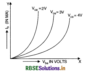
(b) Output Characteristics
A graph showing the relationship between the collector emitter voltage and collector current at constant base curent is called output characteristics of the transistor.
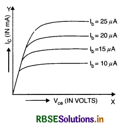
To obtain output characteristics the base current is kept constant at a suitable value the collector-emitter voltage Vce is varied in small steps and the collector current Ic is noted corresponding to each value of the base current Ib. A curve is then plotted between Vce and Ic for a given constant value of Ib. This is one characteristic. Similar characteristic curves can be drawn for different fixed values of Ib (say 10µA, 15 µA, 20 µA etc. as shown in Fig. LAQ 30 (c).
Input resistance is the ratio of change in ∆Vbe to the resulting change in ∆Ib
i.e. Ri = \(\frac{\Delta \mathrm{V}_{b e}}{\Delta \mathrm{I}_b}\)
Current amplification is the ratio of change in collector current to the change in base current for constant Vce
i.e. ß = \(\left(\frac{\Delta \mathrm{I}_{\mathrm{C}}}{\Delta \mathrm{I}_b}\right)_{\mathrm{V}_{c e}}\).
HOTS QUESTIONS
Question 1.
Find the current produced at room temperature in a pure germanium plate of area 2 x 10⁻⁴ m2 and of thickness 1.2 x 10⁻³ m when a potential of 5V is applied across the faces. Concentration of carriers in germanium at room temperature is 1.6 x 10⁶ per cubic meter. The mobilities of electrons and holes are 0.4 m2 V-1s-1 and 0.2 m2 V-1s-1 respectively. How much heat is generated in the plate in 100 s?
Answer:
Current density J = neAvd .........................(i)
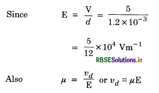
So eq. (i) becomes
J = n e µ E .......................(ii)
For both holes and electron eq. (ii) becomes
J = neE (µe + µh)
or i = JA = neAE (µe + µh)
= 1.6 x 106 x 1.6 x 10-19 x 2 x 10-4 x \(\frac{5}{12}\) x 104 [0.4 + 0.6]
or i = 1.13 x 10⁻¹³ A
∴ Heat generated
H = Vit = 5 x 1.13 x 10-13 x 100
or H = 65 x 10-11 J
Question 2.
In an n-p-n transistor 1010 electrons enter the emitter in 10 s. 2% of electrons are lost in the base. Calculate the current transfer ratio and current amplification factor.
Answer:
Number of electrons entering emitter per second ne = 1010
Number of electrons reaching from emitter to collector
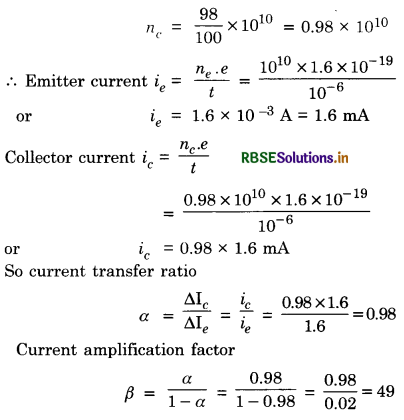
Question 3.
A 10V zener diode along with a series resistance is connected across a 40V supply. Calculate the minimum value of the resistance required, if the maximum zener current is 50 mA.
Answer:
From the figure HQ 3 we find that
Vi = 40V, I1 = 50 mA
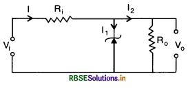
∴ Maximum current
I = I1 + I2 = 5mA + 0
= 50 mA = 50 x 10-3 A
Since maximum current flows through zener diode, hence
I2 = 0
Voltage drop across zener, V0 = 10 V
Since I is maximum, hence maximum value of R is given by
R = \(\frac{\mathrm{V}_i-\mathrm{V}_0}{\mathrm{I}}=\frac{40-10}{50 \times 10^{-3}}\) = 60Ω
Question 4.
A silicon transistor amplifier circuit is given below. If current amplfication factor ß = 100, determine
(а) Base current Ib
(b) Collector current Ic
(c) Collector emitter voltage
(d) Collector base voltage.
Take voltage drop between base and emitter as 0.7 V
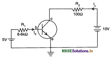
Answer:
(a) Here Vbe = 0.7V
Applying Kirchhoffs 2nd law in base-emitter closed circuit
5 = R1Ib + Vbe
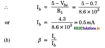
∴ Ic = ßIb = 100 x 0.5 = 50 mA
(c) Applying Kirchhoffs 2nd law in collector-emitter closed circuit
10 = R2Ic + Vce
∴ Vce = 10 - R2Ic = 10 - 100 x 50 x 10-3
Vce = 10 - 5 = 5V
(d) Applying voltage addition law of series element (Vc > Ve)
Vce = Vcp + Vbe
∴ Vcb = Vce - Vbe = 5 - 0.7
or Vcb = 4.3 V
Question 5.
In a silicon transistor, the base current is changed by 20 µA. This results in a change of 0.02 V in base to emitter voltage and a change of 2mA in the collector current.
(a) Find the input resistance, ßac and transconductance of the transistor gm.
(b) This transistor is used as an amplifier in CE configuration with load resistance 5kΩ. What is the voltage gain of the amplifier?
Answer:
Here, ∆Ib = 20 µA = 20 x 10-6 A = 0.020 mA, ∆Vbe = 0.02 V, ∆Ic = 2mA
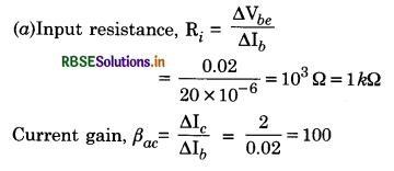
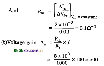
As there is a phase shift of 180° (in CE amplifer) between input and output voltages
∴ AV = -500

- RBSE Class 12 Physics Notes Chapter 2 स्थिर वैद्युत विभव तथा धारिता
- RBSE Class 12 Physics Notes Chapter 3 विद्युत धारा
- RBSE Class 12 Physics Notes Chapter 4 गतिमान आवेश और चुंबकत्व
- RBSE Class 12 Physics Notes Chapter 5 चुंबकत्व एवं द्रव्य
- RBSE Class 12 Physics Notes Chapter 6 वैद्युत चुंबकीय प्रेरण
- RBSE Class 12 Physics Notes Chapter 7 प्रत्यावर्ती धारा
- RBSE Class 12 Physics Notes Chapter 8 वैद्युतचुंबकीय तरंगें
- RBSE Class 12 Physics Notes Chapter 9 किरण प्रकाशिकी एवं प्रकाशिक यंत्र
- RBSE Class 12 Physics Notes Chapter 10 तरंग-प्रकाशिकी
- RBSE Class 12 Physics Notes Chapter 11 विकिरण तथा द्रव्य की द्वैत प्रकृति
- RBSE Class 12 Physics Notes Chapter 12 परमाणु